
Microscopy is the technical field of using microscopes to view objects and areas of objects that cannot be seen with the naked eye. There are three well-known branches of microscopy: optical, electron, and scanning probe microscopy, along with the emerging field of X-ray microscopy.

Holography is a technique that enables a wavefront to be recorded and later reconstructed. It is best known as a method of generating three-dimensional images, and has a wide range of other uses, including data storage, microscopy, and interferometry. In principle, it is possible to make a hologram for any type of wave.
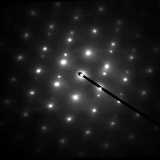
Electron diffraction is a generic term for phenomena associated with changes in the direction of electron beams due to elastic interactions with atoms. It occurs due to elastic scattering, when there is no change in the energy of the electrons. The negatively charged electrons are scattered due to Coulomb forces when they interact with both the positively charged atomic core and the negatively charged electrons around the atoms. The resulting map of the directions of the electrons far from the sample is called a diffraction pattern, see for instance Figure 1. Beyond patterns showing the directions of electrons, electron diffraction also plays a major role in the contrast of images in electron microscopes.
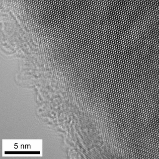
High-resolution transmission electron microscopy is an imaging mode of specialized transmission electron microscopes that allows for direct imaging of the atomic structure of samples. It is a powerful tool to study properties of materials on the atomic scale, such as semiconductors, metals, nanoparticles and sp2-bonded carbon. While this term is often also used to refer to high resolution scanning transmission electron microscopy, mostly in high angle annular dark field mode, this article describes mainly the imaging of an object by recording the two-dimensional spatial wave amplitude distribution in the image plane, similar to a "classic" light microscope. For disambiguation, the technique is also often referred to as phase contrast transmission electron microscopy, although this term is less appropriate. At present, the highest point resolution realised in high resolution transmission electron microscopy is around 0.5 ångströms (0.050 nm). At these small scales, individual atoms of a crystal and defects can be resolved. For 3-dimensional crystals, it is necessary to combine several views, taken from different angles, into a 3D map. This technique is called electron tomography.
Holographic interferometry (HI) is a technique which enables static and dynamic displacements of objects with optically rough surfaces to be measured to optical interferometric precision. These measurements can be applied to stress, strain and vibration analysis, as well as to non-destructive testing and radiation dosimetry. It can also be used to detect optical path length variations in transparent media, which enables, for example, fluid flow to be visualised and analyzed. It can also be used to generate contours representing the form of the surface.
Digital holography refers to the acquisition and processing of holograms with a digital sensor array, typically a CCD camera or a similar device. Image rendering, or reconstruction of object data is performed numerically from digitized interferograms. Digital holography offers a means of measuring optical phase data and typically delivers three-dimensional surface or optical thickness images. Several recording and processing schemes have been developed to assess optical wave characteristics such as amplitude, phase, and polarization state, which make digital holography a very powerful method for metrology applications .
Computer-generated holography (CGH) is a technique that uses computer algorithms to generate holograms. It involves generating holographic interference patterns. A computer-generated hologram can be displayed on a dynamic holographic display, or it can be printed onto a mask or film using lithography. When a hologram is printed onto a mask or film, it is then illuminated by a coherent light source to display the holographic images.
Low-energy electron microscopy, or LEEM, is an analytical surface science technique used to image atomically clean surfaces, atom-surface interactions, and thin (crystalline) films. In LEEM, high-energy electrons are emitted from an electron gun, focused using a set of condenser optics, and sent through a magnetic beam deflector. The “fast” electrons travel through an objective lens and begin decelerating to low energies near the sample surface because the sample is held at a potential near that of the gun. The low-energy electrons are now termed “surface-sensitive” and the near-surface sampling depth can be varied by tuning the energy of the incident electrons. The low-energy elastically backscattered electrons travel back through the objective lens, reaccelerate to the gun voltage, and pass through the beam separator again. However, now the electrons travel away from the condenser optics and into the projector lenses. Imaging of the back focal plane of the objective lens into the object plane of the projector lens produces a diffraction pattern at the imaging plane and recorded in a number of different ways. The intensity distribution of the diffraction pattern will depend on the periodicity at the sample surface and is a direct result of the wave nature of the electrons. One can produce individual images of the diffraction pattern spot intensities by turning off the intermediate lens and inserting a contrast aperture in the back focal plane of the objective lens, thus allowing for real-time observations of dynamic processes at surfaces. Such phenomena include : tomography, phase transitions, adsorption, reaction, segregation, thin film growth, etching, strain relief, sublimation, and magnetic microstructure. These investigations are only possible because of the accessibility of the sample; allowing for a wide variety of in situ studies over a wide temperature range. LEEM was invented by Ernst Bauer in 1962; however, not fully developed until 1985.
A holographic display is a type of 3D display that utilizes light diffraction to display a three-dimensional image to the viewer. Holographic displays are distinguished from other forms of 3D displays in that they do not require the viewer to wear any special glasses or use external equipment to be able to see the image, and do not cause the vergence-accommodation conflict.

Ptychography is a computational method of microscopic imaging. It generates images by processing many coherent interference patterns that have been scattered from an object of interest. Its defining characteristic is translational invariance, which means that the interference patterns are generated by one constant function moving laterally by a known amount with respect to another constant function. The interference patterns occur some distance away from these two components, so that the scattered waves spread out and "fold" into one another as shown in the figure.
Electronic quantum holography is an information storage technology which can encode and read out data at unprecedented density storing as much as 35 bits per electron.

The contrast transfer function (CTF) mathematically describes how aberrations in a transmission electron microscope (TEM) modify the image of a sample. This contrast transfer function (CTF) sets the resolution of high-resolution transmission electron microscopy (HRTEM), also known as phase contrast TEM.
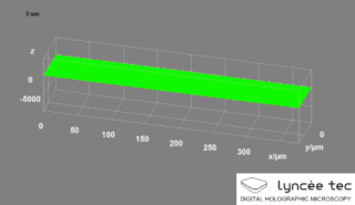
Digital holographic microscopy (DHM) is digital holography applied to microscopy. Digital holographic microscopy distinguishes itself from other microscopy methods by not recording the projected image of the object. Instead, the light wave front information originating from the object is digitally recorded as a hologram, from which a computer calculates the object image by using a numerical reconstruction algorithm. The image forming lens in traditional microscopy is thus replaced by a computer algorithm. Other closely related microscopy methods to digital holographic microscopy are interferometric microscopy, optical coherence tomography and diffraction phase microscopy. Common to all methods is the use of a reference wave front to obtain amplitude (intensity) and phase information. The information is recorded on a digital image sensor or by a photodetector from which an image of the object is created (reconstructed) by a computer. In traditional microscopy, which do not use a reference wave front, only intensity information is recorded and essential information about the object is lost.
Electron magnetic circular dichroism (EMCD) is the EELS equivalent of XMCD.
A common-path interferometer is a class of interferometers in which the reference beam and sample beams travel along the same path. Examples include the Sagnac interferometer, Zernike phase-contrast interferometer, and the point diffraction interferometer. A common-path interferometer is generally more robust to environmental vibrations than a "double-path interferometer" such as the Michelson interferometer or the Mach–Zehnder interferometer. Although travelling along the same path, the reference and sample beams may travel along opposite directions, or they may travel along the same direction but with the same or different polarization.
Holographic interference microscopy (HIM) is holographic interferometry applied for microscopy for visualization of phase micro-objects. Phase micro-objects are invisible because they do not change intensity of light, they insert only invisible phase shifts. The holographic interference microscopy distinguishes itself from other microscopy methods by using a hologram and the interference for converting invisible phase shifts into intensity changes.

Quantitative phase contrast microscopy or quantitative phase imaging are the collective names for a group of microscopy methods that quantify the phase shift that occurs when light waves pass through a more optically dense object.
The time-domain counterpart of spatial holography is called time-domain holography. In other words, the principles of spatial holography is surveyed in time domain. Time-domain holography was inspired by the theory known as space-time duality which was introduced by Brian H. Kolner in 1994.
Joanne Etheridge is an Australian physicist. She is Director of the Monash Centre for Electron Microscopy and Professor in the Department of Materials Science and Engineering at Monash University.
4D scanning transmission electron microscopy is a subset of scanning transmission electron microscopy (STEM) which utilizes a pixelated electron detector to capture a convergent beam electron diffraction (CBED) pattern at each scan location. This technique captures a 2 dimensional reciprocal space image associated with each scan point as the beam rasters across a 2 dimensional region in real space, hence the name 4D STEM. Its development was enabled by evolution in STEM detectors and improvements computational power. The technique has applications in visual diffraction imaging, phase orientation and strain mapping, phase contrast analysis, among others.


