Molecular scale electronics

Last updated

Molecular scale electronics, also called single-molecule electronics, is a branch of nanotechnology that uses single molecules, or nanoscale collections of single molecules, as electronic components. Because single molecules constitute the smallest stable structures imaginable[ citation needed ], this miniaturization is the ultimate goal for shrinking electrical circuits.

Contents

The field is often termed simply as "molecular electronics", but this term is also used to refer to the distantly related field of conductive polymers and organic electronics, which uses the properties of molecules to affect the bulk properties of a material. A nomenclature distinction has been suggested so that molecular materials for electronics refers to this latter field of bulk applications, while molecular scale electronics refers to the nanoscale single-molecule applications treated here. [1] [2]

Fundamental concepts

Conventional electronics have traditionally been made from bulk materials. Ever since their invention in 1958, the performance and complexity of integrated circuits has undergone exponential growth, a trend named Moore’s law, as feature sizes of the embedded components have shrunk accordingly. As the structures shrink, the sensitivity to deviations increases. In a few technology generations, the composition of the devices must be controlled to a precision of a few atoms [3] for the devices to work. With bulk methods growing increasingly demanding and costly as they near inherent limits, the idea was born that the components could instead be built up atom by atom in a chemistry lab (bottom up) versus carving them out of bulk material (top down). This is the idea behind molecular electronics, with the ultimate miniaturization being components contained in single molecules.

In single-molecule electronics, the bulk material is replaced by single molecules. Instead of forming structures by removing or applying material after a pattern scaffold, the atoms are put together in a chemistry lab. In this way, billions of billions of copies are made simultaneously (typically more than 1020 molecules are made at once) while the composition of molecules are controlled down to the last atom. The molecules used have properties that resemble traditional electronic components such as a wire, transistor or rectifier.

Single-molecule electronics is an emerging field, and entire electronic circuits consisting exclusively of molecular sized compounds are still very far from being realized.[ citation needed ] However, the unceasing demand for more computing power, along with the inherent limits of lithographic methods as of 2016, make the transition seem unavoidable. Currently, the focus is on discovering molecules with interesting properties and on finding ways to obtain reliable and reproducible contacts between the molecular components and the bulk material of the electrodes.[ citation needed ]

Theoretical basis

Molecular electronics operates at of distances less than 100 nanometers. The miniaturization down to single molecules brings the scale down to a regime where quantum mechanics effects are important. In conventional electronic components, electrons can be filled in or drawn out more or less like a continuous flow of electric charge. In contrast, in molecular electronics the transfer of one electron alters the system significantly. For example, when an electron has been transferred from a source electrode to a molecule, the molecule gets charged up, which makes it far harder for the next electron to transfer (see also Coulomb blockade). The significant amount of energy due to charging must be accounted for when making calculations about the electronic properties of the setup, and is highly sensitive to distances to conducting surfaces nearby.

The theory of single-molecule devices is especially interesting since the system under consideration is an open quantum system in nonequilibrium (driven by voltage). In the low bias voltage regime, the nonequilibrium nature of the molecular junction can be ignored, and the current-voltage traits of the device can be calculated using the equilibrium electronic structure of the system. However, in stronger bias regimes a more sophisticated treatment is required, as there is no longer a variational principle. In the elastic tunneling case (where the passing electron does not exchange energy with the system), the formalism of Rolf Landauer can be used to calculate the transmission through the system as a function of bias voltage, and hence the current. In inelastic tunneling, an elegant formalism based on the non-equilibrium Green's functions of Leo Kadanoff and Gordon Baym, and independently by Leonid Keldysh was advanced by Ned Wingreen and Yigal Meir. This Meir-Wingreen formulation has been used to great success in the molecular electronics community to examine the more difficult and interesting cases where the transient electron exchanges energy with the molecular system (for example through electron-phonon coupling or electronic excitations).

Further, connecting single molecules reliably to a larger scale circuit has proven a great challenge, and constitutes a significant hindrance to commercialization.

Examples

Common for molecules used in molecular electronics is that the structures contain many alternating double and single bonds (see also Conjugated system). This is done because such patterns delocalize the molecular orbitals, making it possible for electrons to move freely over the conjugated area.

Wires

This animation of a rotating carbon nanotube shows its 3D structure. Kohlenstoffnanoroehre Animation.gif
This animation of a rotating carbon nanotube shows its 3D structure.

The sole purpose of molecular wires is to electrically connect different parts of a molecular electrical circuit. As the assembly of these and their connection to a macroscopic circuit is still not mastered, the focus of research in single-molecule electronics is primarily on the functionalized molecules: molecular wires are characterized by containing no functional groups and are hence composed of plain repetitions of a conjugated building block. Among these are the carbon nanotubes that are quite large compared to the other suggestions but have shown very promising electrical properties.

The main problem with the molecular wires is to obtain good electrical contact with the electrodes so that electrons can move freely in and out of the wire.

Transistors

Single-molecule transistors are fundamentally different from the ones known from bulk electronics. The gate in a conventional (field-effect) transistor determines the conductance between the source and drain electrode by controlling the density of charge carriers between them, whereas the gate in a single-molecule transistor controls the possibility of a single electron to jump on and off the molecule by modifying the energy of the molecular orbitals. One of the effects of this difference is that the single-molecule transistor is almost binary: it is either on or off. This opposes its bulk counterparts, which have quadratic responses to gate voltage.

It is the quantization of charge into electrons that is responsible for the markedly different behavior compared to bulk electronics. Because of the size of a single molecule, the charging due to a single electron is significant and provides means to turn a transistor on or off (see Coulomb blockade). For this to work, the electronic orbitals on the transistor molecule cannot be too well integrated with the orbitals on the electrodes. If they are, an electron cannot be said to be located on the molecule or the electrodes and the molecule will function as a wire.

A popular group of molecules, that can work as the semiconducting channel material in a molecular transistor, is the oligopolyphenylenevinylenes (OPVs) that works by the Coulomb blockade mechanism when placed between the source and drain electrode in an appropriate way. [4] Fullerenes work by the same mechanism and have also been commonly used.

Semiconducting carbon nanotubes have also been demonstrated to work as channel material but although molecular, these molecules are sufficiently large to behave almost as bulk semiconductors.

The size of the molecules, and the low temperature of the measurements being conducted, makes the quantum mechanical states well defined. Thus, it is being researched if the quantum mechanical properties can be used for more advanced purposes than simple transistors (e.g. spintronics).

Physicists at the University of Arizona, in collaboration with chemists from the University of Madrid, have designed a single-molecule transistor using a ring-shaped molecule similar to benzene. Physicists at Canada's National Institute for Nanotechnology have designed a single-molecule transistor using styrene. Both groups expect (the designs were experimentally unverified as of June 2005) their respective devices to function at room temperature, and to be controlled by a single electron. [5]

Rectifiers (diodes)

Hydrogen can be removed from individual tetraphenylporphyrin (H2TPP) molecules by applying excess voltage to the tip of a scanning tunneling microscope (STAM, a); this removal alters the current-voltage (I-V) curves of TPP molecules, measured using the same STM tip, from diode-like (red curve in b) to resistor-like (green curve). Image (c) shows a row of TPP, H2TPP and TPP molecules. While scanning image (d), excess voltage was applied to H2TPP at the black dot, which instantly removed hydrogen, as shown in the bottom part of (d) and in the re-scan image (e). Such manipulations can be used in single-molecule electronics. Dehydrogenation of H2TPP by STM.jpg
Hydrogen can be removed from individual tetraphenylporphyrin (H2TPP) molecules by applying excess voltage to the tip of a scanning tunneling microscope (STAM, a); this removal alters the current-voltage (I-V) curves of TPP molecules, measured using the same STM tip, from diode-like (red curve in b) to resistor-like (green curve). Image (c) shows a row of TPP, H2TPP and TPP molecules. While scanning image (d), excess voltage was applied to H2TPP at the black dot, which instantly removed hydrogen, as shown in the bottom part of (d) and in the re-scan image (e). Such manipulations can be used in single-molecule electronics.

Molecular rectifiers are mimics of their bulk counterparts and have an asymmetric construction so that the molecule can accept electrons in one end but not the other. The molecules have an electron donor (D) in one end and an electron acceptor (A) in the other. This way, the unstable state D+ – A will be more readily made than D – A+. The result is that an electric current can be drawn through the molecule if the electrons are added through the acceptor end, but less easily if the reverse is attempted.

Methods

One of the biggest problems with measuring on single molecules is to establish reproducible electrical contact with only one molecule and doing so without shortcutting the electrodes. Because the current photolithographic technology is unable to produce electrode gaps small enough to contact both ends of the molecules tested (on the order of nanometers), alternative strategies are applied.

Molecular gaps

One way to produce electrodes with a molecular sized gap between them is break junctions, in which a thin electrode is stretched until it breaks. Another is electromigration. Here a current is led through a thin wire until it melts and the atoms migrate to produce the gap. Further, the reach of conventional photolithography can be enhanced by chemically etching or depositing metal on the electrodes.

Probably the easiest way to conduct measurements on several molecules is to use the tip of a scanning tunneling microscope (STM) to contact molecules adhered at the other end to a metal substrate. [7]

Anchoring

A popular way to anchor molecules to the electrodes is to make use of sulfur's high chemical affinity to gold. In these setups, the molecules are synthesized so that sulfur atoms are placed strategically to function as crocodile clips connecting the molecules to the gold electrodes. Though useful, the anchoring is non-specific and thus anchors the molecules randomly to all gold surfaces. Further, the contact resistance is highly dependent on the precise atomic geometry around the site of anchoring and thereby inherently compromises the reproducibility of the connection.

To circumvent the latter issue, experiments has shown that fullerenes could be a good candidate for use instead of sulfur because of the large conjugated π-system that can electrically contact many more atoms at once than one atom of sulfur. [8]

Fullerene nanoelectronics

In polymers, classical organic molecules are composed of both carbon and hydrogen (and sometimes additional compounds such as nitrogen, chlorine or sulphur). They are obtained from petrol and can often be synthesized in large amounts. Most of these molecules are insulating when their length exceeds a few nanometers. However, naturally occurring carbon is conducting, especially graphite recovered from coal or encountered otherwise. From a theoretical viewpoint, graphite is a semi-metal, a category in between metals and semi-conductors. It has a layered structure, each sheet being one atom thick. Between each sheet, the interactions are weak enough to allow an easy manual cleavage.

Tailoring the graphite sheet to obtain well defined nanometer-sized objects remains a challenge. However, by the close of the twentieth century, chemists were exploring methods to fabricate extremely small graphitic objects that could be considered single molecules. After studying the interstellar conditions under which carbon is known to form clusters, Richard Smalley's group (Rice University, Texas) set up an experiment in which graphite was vaporized via laser irradiation. Mass spectrometry revealed that clusters containing specific magic numbers of atoms were stable, especially those clusters of 60 atoms. Harry Kroto, an English chemist who assisted in the experiment, suggested a possible geometry for these clusters – atoms covalently bound with the exact symmetry of a soccer ball. Coined buckminsterfullerenes, buckyballs, or C60, the clusters retained some properties of graphite, such as conductivity. These objects were rapidly envisioned as possible building blocks for molecular electronics.

Problems

Artifacts

When trying to measure electronic traits of molecules, artificial phenomena can occur that can be hard to distinguish from truly molecular behavior. [9] Before they were discovered, these artifacts have mistakenly been published as being features pertaining to the molecules in question.

Applying a voltage drop on the order of volts across a nanometer sized junction results in a very strong electrical field. The field can cause metal atoms to migrate and eventually close the gap by a thin filament, which can be broken again when carrying a current. The two levels of conductance imitate molecular switching between a conductive and an isolating state of a molecule.

Another encountered artifact is when the electrodes undergo chemical reactions due to the high field strength in the gap. When the voltage bias is reversed, the reaction will cause hysteresis in the measurements that can be interpreted as being of molecular origin.

A metallic grain between the electrodes can act as a single electron transistor by the mechanism described above, thus resembling the traits of a molecular transistor. This artifact is especially common with nanogaps produced by the electromigration method.

Commercialization

One of the biggest hindrances for single-molecule electronics to be commercially exploited is the lack of methods to connect a molecular sized circuit to bulk electrodes in a way that gives reproducible results. At the current state, the difficulty of connecting single molecules vastly outweighs any possible performance increase that could be gained from such shrinkage. The difficulties grow worse if the molecules are to have a certain spatial orientation and/or have multiple poles to connect.

Also problematic is that some measurements on single molecules are carried out in cryogenic temperatures (near absolute zero), which is very energy consuming. This is done to reduce signal noise enough to measure the faint currents of single molecules.

History and recent progress

Graphical representation of a rotaxane, useful as a molecular switch Rotaxane cartoon.jpg
Graphical representation of a rotaxane, useful as a molecular switch

In their treatment of so-called donor-acceptor complexes in the 1940s, Robert Mulliken and Albert Szent-Györgyi advanced the concept of charge transfer in molecules. They subsequently further refined the study of both charge transfer and energy transfer in molecules. Likewise, a 1974 paper from Mark Ratner and Ari Aviram illustrated a theoretical molecular rectifier. [10]

In 1988, Aviram described in detail a theoretical single-molecule field-effect transistor. Further concepts were proposed by Forrest Carter of the Naval Research Laboratory, including single-molecule logic gates. A wide range of ideas were presented, under his aegis, at a conference entitled Molecular Electronic Devices in 1988. [11] These were theoretical constructs and not concrete devices. The direct measurement of the electronic traits of individual molecules awaited the development of methods for making molecular-scale electrical contacts. This was no easy task. Thus, the first experiment directly-measuring the conductance of a single molecule was only reported in 1995 on a single C60 molecule by C. Joachim and J. K. Gimzewsky in their seminal Physical Review Letter paper and later in 1997 by Mark Reed and co-workers on a few hundred molecules. Since then, this branch of the field has advanced rapidly. Likewise, as it has grown possible to measure such properties directly, the theoretical predictions of the early workers have been confirmed substantially.

The concept of molecular electronics was published in 1974 when Aviram and Ratner suggested an organic molecule that could work as a rectifier. [12] Having both huge commercial and fundamental interest, much effort was put into proving its feasibility, and 16 years later in 1990, the first demonstration of an intrinsic molecular rectifier was realized by Ashwell and coworkers for a thin film of molecules.

The first measurement of the conductance of a single molecule was realised in 1994 by C. Joachim and J. K. Gimzewski and published in 1995 (see the corresponding Phys. Rev. Lett. paper). This was the conclusion of 10 years of research started at IBM TJ Watson, using the scanning tunnelling microscope tip apex to switch a single molecule as already explored by A. Aviram, C. Joachim and M. Pomerantz at the end of the 1980s (see their seminal Chem. Phys. Lett. paper during this period). The trick was to use a UHV Scanning Tunneling microscope to allow the tip apex to gently touch the top of a single C
60
molecule adsorbed on an Au(110) surface. A resistance of 55 MOhms was recorded along with a low voltage linear I-V. The contact was certified by recording the I-z current distance property, which allows measurement of the deformation of the C
60
cage under contact. This first experiment was followed by the reported result using a mechanical break junction method to connect two gold electrodes to a sulfur-terminated molecular wire by Mark Reed and James Tour in 1997. [13]

Recent progress in nanotechnology and nanoscience has facilitated both experimental and theoretical study of molecular electronics. Development of the scanning tunneling microscope (STM) and later the atomic force microscope (AFM) have greatly facilitated manipulating single-molecule electronics. Also, theoretical advances in molecular electronics have facilitated further understanding of non-adiabatic charge transfer events at electrode-electrolyte interfaces. [14] [15]

A single-molecule amplifier was implemented by C. Joachim and J.K. Gimzewski in IBM Zurich. This experiment, involving one C
60
molecule, demonstrated that one such molecule can provide gain in a circuit via intramolecular quantum interference effects alone.

A collaboration of researchers at Hewlett-Packard (HP) and University of California, Los Angeles (UCLA), led by James Heath, Fraser Stoddart, R. Stanley Williams, and Philip Kuekes, has developed molecular electronics based on rotaxanes and catenanes.

Work is also occurring on the use of single-wall carbon nanotubes as field-effect transistors. Most of this work is being done by International Business Machines (IBM).

Some specific reports of a field-effect transistor based on molecular self-assembled monolayers were shown to be fraudulent in 2002 as part of the Schön scandal. [16]

Until recently entirely theoretical, the Aviram-Ratner model for a unimolecular rectifier has been confirmed unambiguously in experiments by a group led by Geoffrey J. Ashwell at Bangor University, UK. [17] [18] [19] Many rectifying molecules have so far been identified, and the number and efficiency of these systems is growing rapidly.

Supramolecular electronics is a new field involving electronics at a supramolecular level.

An important issue in molecular electronics is the determination of the resistance of a single molecule (both theoretical and experimental). For example, Bumm, et al. used STM to analyze a single molecular switch in a self-assembled monolayer to determine how conductive such a molecule can be. [20] Another problem faced by this field is the difficulty of performing direct characterization since imaging at the molecular scale is often difficult in many experimental devices.

See also

Related Research Articles

<span class="mw-page-title-main">Cathode ray</span> Beam of electrons observed in vacuum tubes

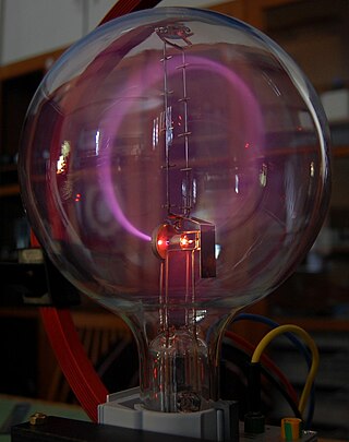
Cathode rays or electron beams (e-beam) are streams of electrons observed in discharge tubes. If an evacuated glass tube is equipped with two electrodes and a voltage is applied, glass behind the positive electrode is observed to glow, due to electrons emitted from the cathode. They were first observed in 1859 by German physicist Julius Plücker and Johann Wilhelm Hittorf, and were named in 1876 by Eugen Goldstein Kathodenstrahlen, or cathode rays. In 1897, British physicist J. J. Thomson showed that cathode rays were composed of a previously unknown negatively charged particle, which was later named the electron. Cathode-ray tubes (CRTs) use a focused beam of electrons deflected by electric or magnetic fields to render an image on a screen.

Molecular electronics is the study and application of molecular building blocks for the fabrication of electronic components. It is an interdisciplinary area that spans physics, chemistry, and materials science. The unifying feature is use of molecular building blocks to fabricate electronic components. Due to the prospect of size reduction in electronics offered by molecular-level control of properties, molecular electronics has generated much excitement. It provides a potential means to extend Moore's Law beyond the foreseen limits of small-scale conventional silicon integrated circuits.

A nanowire is a nanostructure in the form of a wire with the diameter of the order of a nanometre. More generally, nanowires can be defined as structures that have a thickness or diameter constrained to tens of nanometers or less and an unconstrained length. At these scales, quantum mechanical effects are important—which coined the term "quantum wires".

<span class="mw-page-title-main">Conductive polymer</span> Organic polymers that conduct electricity

Conductive polymers or, more precisely, intrinsically conducting polymers (ICPs) are organic polymers that conduct electricity. Such compounds may have metallic conductivity or can be semiconductors. The main advantage of conductive polymers is that they are easy to process, mainly by dispersion. Conductive polymers are generally not thermoplastics, i.e., they are not thermoformable. But, like insulating polymers, they are organic materials. They can offer high electrical conductivity but do not show similar mechanical properties to other commercially available polymers. The electrical properties can be fine-tuned using the methods of organic synthesis and by advanced dispersion techniques.

Organic semiconductors are solids whose building blocks are pi-bonded molecules or polymers made up by carbon and hydrogen atoms and – at times – heteroatoms such as nitrogen, sulfur and oxygen. They exist in the form of molecular crystals or amorphous thin films. In general, they are electrical insulators, but become semiconducting when charges are either injected from appropriate electrodes, upon doping or by photoexcitation.

<span class="mw-page-title-main">Breakdown voltage</span> Voltage at which insulator becomes conductive

The breakdown voltage of an insulator is the minimum voltage that causes a portion of an insulator to experience electrical breakdown and become electrically conductive.

<span class="mw-page-title-main">Electronic component</span> Discrete device in an electronic system

An electronic component is any basic discrete electronic device or physical entity part of an electronic system used to affect electrons or their associated fields. Electronic components are mostly industrial products, available in a singular form and are not to be confused with electrical elements, which are conceptual abstractions representing idealized electronic components and elements. A datasheet for an electronic component is a technical document that provides detailed information about the component's specifications, characteristics, and performance.

A break junction is an electronic device which consists of two metal wires separated by a very thin gap, on the order of the inter-atomic spacing. This can be done by physically pulling the wires apart or through chemical etching or electromigration. As the wire breaks, the separation between the electrodes can be indirectly controlled by monitoring the electrical resistance of the junction.

<span class="mw-page-title-main">Unimolecular rectifier</span>

A unimolecular rectifier is a single organic molecule which functions as a rectifier of electric current. The idea was first proposed in 1974 by Arieh Aviram, then at IBM, and Mark Ratner, then at New York University. Their publication was the first serious and concrete theoretical proposal in the new field of molecular electronics (UE). Based on the mesomeric effect of certain chemical compounds on organic molecules, a molecular rectifier was built by simulating the pn junction with the help of chemical compounds.

Nanoelectronics refers to the use of nanotechnology in electronic components. The term covers a diverse set of devices and materials, with the common characteristic that they are so small that inter-atomic interactions and quantum mechanical properties need to be studied extensively. Some of these candidates include: hybrid molecular/semiconductor electronics, one-dimensional nanotubes/nanowires or advanced molecular electronics.

<span class="mw-page-title-main">Mesoscopic physics</span> Subdiscipline of condensed matter physics that deals with materials of an intermediate size

Mesoscopic physics is a subdiscipline of condensed matter physics that deals with materials of an intermediate size. These materials range in size between the nanoscale for a quantity of atoms and of materials measuring micrometres. The lower limit can also be defined as being the size of individual atoms. At the microscopic scale are bulk materials. Both mesoscopic and macroscopic objects contain many atoms. Whereas average properties derived from constituent materials describe macroscopic objects, as they usually obey the laws of classical mechanics, a mesoscopic object, by contrast, is affected by thermal fluctuations around the average, and its electronic behavior may require modeling at the level of quantum mechanics.

<span class="mw-page-title-main">Mark Ratner</span> American physical chemist

Mark A. Ratner is an American chemist and professor emeritus at Northwestern University whose work focuses on the interplay between molecular structure and molecular properties. He is widely credited as the "father of molecular-scale electronics" thanks to his groundbreaking work with Arieh Aviram in 1974 that first envisioned how electronic circuit elements might be constructed from single molecules and how these circuits might behave.

Nanofluidic circuitry is a nanotechnology aiming for control of fluids in nanometer scale. Due to the effect of an electrical double layer within the fluid channel, the behavior of nanofluid is observed to be significantly different compared with its microfluidic counterparts. Its typical characteristic dimensions fall within the range of 1–100 nm. At least one dimension of the structure is in nanoscopic scale. Phenomena of fluids in nano-scale structure are discovered to be of different properties in electrochemistry and fluid dynamics.

A chemically modified electrode is an electrical conductor that has its surface modified for different electrochemical functions. Chemically modified electrodes are made using advanced approaches to electrode systems by adding a thin film or layer of certain chemicals to change properties of the conductor according to its targeted function.

<span class="mw-page-title-main">Field-effect transistor</span> Type of transistor

The field-effect transistor (FET) is a type of transistor that uses an electric field to control the flow of current in a semiconductor. It comes in two types: junction FET (JFET) and metal-oxide-semiconductor FET (MOSFET). FETs have three terminals: source, gate, and drain. FETs control the flow of current by the application of a voltage to the gate, which in turn alters the conductivity between the drain and source.

Double-layer capacitance is the important characteristic of the electrical double layer which appears at the interface between a surface and a fluid. At this boundary two layers of electric charge with opposing polarity form, one at the surface of the electrode, and one in the electrolyte. These two layers, electrons on the electrode and ions in the electrolyte, are typically separated by a single layer of solvent molecules that adhere to the surface of the electrode and act like a dielectric in a conventional capacitor. The amount of charge stored in double-layer capacitor depends on the applied voltage.

Potential graphene applications include lightweight, thin, and flexible electric/photonics circuits, solar cells, and various medical, chemical and industrial processes enhanced or enabled by the use of new graphene materials.

Band-gap engineering is the process of controlling or altering the band gap of a material. This is typically done to semiconductors by controlling the composition of alloys, constructing layered materials with alternating compositions, or by inducing strain either epitaxially or topologically. A band gap is the range in a solid where no electron state can exist. The band gap of insulators is much larger than in semiconductors. Conductors or metals have a much smaller or nonexistent band gap than semiconductors since the valence and conduction bands overlap. Controlling the band gap allows for the creation of desirable electrical properties.

<span class="mw-page-title-main">Chemiresistor</span> Material with changing electrical resistance according to its surroundings

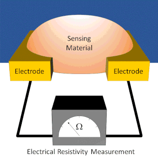
A chemiresistor is a material that changes its electrical resistance in response to changes in the nearby chemical environment. Chemiresistors are a class of chemical sensors that rely on the direct chemical interaction between the sensing material and the analyte. The sensing material and the analyte can interact by covalent bonding, hydrogen bonding, or molecular recognition. Several different materials have chemiresistor properties: semiconducting metal oxides, some conductive polymers, and nanomaterials like graphene, carbon nanotubes and nanoparticles. Typically these materials are used as partially selective sensors in devices like electronic tongues or electronic noses.

This glossary of nanotechnology is a list of definitions of terms and concepts relevant to nanotechnology, its sub-disciplines, and related fields.

References

  1. Petty, M.C.; Bryce, M.R. & Bloor, D. (1995). Introduction to Molecular Electronics. New York: Oxford University Press. pp. 1–25. ISBN   978-0-19-521156-6.
  2. Tour, James M.; et al. (1998). "Recent advances in molecular scale electronics". Annals of the New York Academy of Sciences . 852 (1): 197–204. Bibcode:1998NYASA.852..197T. CiteSeerX   10.1.1.506.4411 . doi:10.1111/j.1749-6632.1998.tb09873.x. S2CID   18011089.
  3. Waser, Rainer; Lüssem, B. & Bjørnholm, T. (2008). "Chapter 8: Concepts in Single-Molecule Electronics". Nanotechnology. Volume 4: Information Technology II. Weinheim: Wiley-VCH Verlag GmbH & Co. KGaA. pp. 175–212. ISBN   978-3-527-31737-0.
  4. Kubatkin, S.; et al. (2003). "Single-electron transistor of a single organic molecule with access to several redox states". Nature. 425 (6959): 698–701. Bibcode:2003Natur.425..698K. doi:10.1038/nature02010. PMID   14562098. S2CID   495125.
  5. Anderson, Mark (2005-06-09) "Honey, I Shrunk the PC". Wired.com
  6. Zoldan, Vinícius Claudio; Faccio, Ricardo & Pasa, André Avelino (2015). "N and p type character of single molecule diodes". Scientific Reports. 5: 8350. Bibcode:2015NatSR...5E8350Z. doi:10.1038/srep08350. PMC   4322354 . PMID   25666850.
  7. Gimzewski, J.K.; Joachim, C. (1999). "Nanoscale science of single molecules using local probes". Science. 283 (5408): 1683–1688. Bibcode:1999Sci...283.1683G. doi:10.1126/science.283.5408.1683. PMID   10073926.
  8. Sørensen, J.K. Archived 2016-03-29 at the Wayback Machine . (2006). "Synthesis of new components, functionalized with (60)fullerene, for molecular electronics". 4th Annual meeting – CONT 2006, University of Copenhagen.
  9. Service, R.F. (2003). "Molecular electronics – Next-generation technology hits an early midlife crisis". Science. 302 (5645): 556–+. doi:10.1126/science.302.5645.556. PMID   14576398. S2CID   42452751.
  10. Aviram, Arieh; Ratner, Mark A. (1974). "Molecular rectifiers". Chemical Physics Letters. 29 (2): 277–283. Bibcode:1974CPL....29..277A. doi:10.1016/0009-2614(74)85031-1.
  11. Carter, F. L.; Siatkowski, R. E. and Wohltjen, H. (eds.) (1988) Molecular Electronic Devices, pp. 229–244, North Holland, Amsterdam.
  12. Aviram, Arieh; Ratner, M.A. (1974). "Molecular rectifiers". Chemical Physics Letters. 29 (2): 277–283. Bibcode:1974CPL....29..277A. doi:10.1016/0009-2614(74)85031-1.
  13. Reed, M.A.; et al. (1997). "Conductance of a Molecular Junction". Science. 287 (5336): 252–254. doi:10.1126/science.278.5336.252.
  14. Gupta, Chaitanya; Shannon, Mark A.; Kenis, Paul J. A. (2009). "Mechanisms of Charge Transport through Monolayer-Modified Polycrystalline Gold Electrodes in the Absence of Redox-Active Moieties". The Journal of Physical Chemistry C. 113 (11): 4687–4705. doi:10.1021/jp8090045. S2CID   97596654.
  15. Gupta, Chaitanya; Shannon, Mark A.; Kenis, Paul J. A. (2009). "Electronic Properties of a Monolayer−Electrolyte Interface Obtained from Mechanistic Impedance Analysis". The Journal of Physical Chemistry C. 113 (21): 9375–9391. doi:10.1021/jp900918u. S2CID   96943244.
  16. Jacoby, Mitch (27 January 2003). "Molecule-based circuitry revisited". Chemical and Engineering News. Retrieved 24 February 2011.
  17. Ashwell, Geoffrey J.; Hamilton, Richard; High, L. R. Hermann (2003). "Molecular rectification: asymmetric current-voltage curves from self-assembled monolayers of a donor-(n-bridge)-acceptor dye". Journal of Materials Chemistry. 13 (7): 1501. doi:10.1039/B304465N.
  18. Ashwell, Geoffrey J.; Chwialkowska, Anna; High, L. R. Hermann (2004). "Au-S-CnH2n-Q3CNQ: self-assembled monolayers for molecular rectification". Journal of Materials Chemistry. 14 (15): 2389. doi:10.1039/B403942D.
  19. Ashwell, Geoffrey J.; Chwialkowska, Anna; Hermann High, L. R. (2004). "Rectifying Au-S-CnH2n-P3CNQ derivatives". Journal of Materials Chemistry. 14 (19): 2848. doi:10.1039/B411343H.
  20. Bumm, L. A.; Arnold, J. J.; Cygan, M. T.; Dunbar, T. D.; Burgin, T. P.; Jones, L.; Allara, D. L.; Tour, J. M.; Weiss, P. S. (1996). "Are Single Molecular Wires Conducting?". Science. 271 (5256): 1705–1707. Bibcode:1996Sci...271.1705B. doi:10.1126/science.271.5256.1705. S2CID   96354191.