Nanomedicine is the medical application of nanotechnology. Nanomedicine ranges from the medical applications of nanomaterials and biological devices, to nanoelectronic biosensors, and even possible future applications of molecular nanotechnology such as biological machines. Current problems for nanomedicine involve understanding the issues related to toxicity and environmental impact of nanoscale materials.
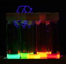
Quantum dots (QDs) or semiconductor nanocrystals are semiconductor particles a few nanometres in size with optical and electronic properties that differ from those of larger particles via quantum mechanical effects. They are a central topic in nanotechnology and materials science. When a quantum dot is illuminated by UV light, an electron in the quantum dot can be excited to a state of higher energy. In the case of a semiconducting quantum dot, this process corresponds to the transition of an electron from the valence band to the conductance band. The excited electron can drop back into the valence band releasing its energy as light. This light emission (photoluminescence) is illustrated in the figure on the right. The color of that light depends on the energy difference between the conductance band and the valence band, or the transition between discrete energy states when the band structure is no longer well-defined in QDs.
Nanomaterials describe, in principle, materials of which a single unit is sized between 1 and 100 nm.

A nanoparticle or ultrafine particle is a particle of matter 1 to 100 nanometres (nm) in diameter. The term is sometimes used for larger particles, up to 500 nm, or fibers and tubes that are less than 100 nm in only two directions. At the lowest range, metal particles smaller than 1 nm are usually called atom clusters instead.

Cadmium selenide is an inorganic compound with the formula CdSe. It is a black to red-black solid that is classified as a II-VI semiconductor of the n-type. It is a pigment, but applications are declining because of environmental concerns.
Hybrid solar cells combine advantages of both organic and inorganic semiconductors. Hybrid photovoltaics have organic materials that consist of conjugated polymers that absorb light as the donor and transport holes. Inorganic materials in hybrid cells are used as the acceptor and electron transporter in the structure. The hybrid photovoltaic devices have a potential for not only low-cost by roll-to-roll processing but also for scalable solar power conversion.
Bis(trimethylsilyl)amine (also known as hexamethyldisilazane and HMDS) is an organosilicon compound with the molecular formula [(CH3)3Si]2NH. The molecule is a derivative of ammonia with trimethylsilyl groups in place of two hydrogen atoms. An electron diffraction study shows that silicon-nitrogen bond length (173.5 pm) and Si-N-Si bond angle (125.5°) to be similar to disilazane (in which methyl groups are replaced by hydrogen atoms) suggesting that steric factors are not a factor in regulating angles in this case. This colorless liquid is a reagent and a precursor to bases that are popular in organic synthesis and organometallic chemistry. Additionally, HMDS is also increasingly used as molecular precursor in chemical vapor deposition techniques to deposit silicon carbonitride thin films or coatings.
A nanocrystalline (NC) material is a polycrystalline material with a crystallite size of only a few nanometers. These materials fill the gap between amorphous materials without any long range order and conventional coarse-grained materials. Definitions vary, but nanocrystalline material is commonly defined as a crystallite (grain) size below 100 nm. Grain sizes from 100 to 500 nm are typically considered "ultrafine" grains.

A quantum dot solar cell (QDSC) is a solar cell design that uses quantum dots as the captivating photovoltaic material. It attempts to replace bulk materials such as silicon, copper indium gallium selenide (CIGS) or cadmium telluride (CdTe). Quantum dots have bandgaps that are adjustable across a wide range of energy levels by changing their size. In bulk materials, the bandgap is fixed by the choice of material(s). This property makes quantum dots attractive for multi-junction solar cells, where a variety of materials are used to improve efficiency by harvesting multiple portions of the solar spectrum.

Bis(trimethylsilyl) sulfide is the chemical compound with the formula ((CH3)3Si)2S. Often abbreviated (tms)2S, this colourless, vile-smelling liquid is a useful aprotic source of "S2−" in chemical synthesis.
Gallium(II) selenide (GaSe) is a chemical compound. It has a hexagonal layer structure, similar to that of GaS. It is a photoconductor, a second harmonic generation crystal in nonlinear optics, and has been used as a far-infrared conversion material at 14–31 THz and above.

Thin-film solar cells are made by depositing one or more thin layers of photovoltaic material onto a substrate, such as glass, plastic or metal. Thin-film solar cells are typically a few nanometers (nm) to a few microns (μm) thick–much thinner than the wafers used in conventional crystalline silicon (c-Si) based solar cells, which can be up to 200 μm thick. Thin-film solar cells are commercially used in several technologies, including cadmium telluride (CdTe), copper indium gallium diselenide (CIGS), and amorphous thin-film silicon.
Silylation is the introduction of one or more (usually) substituted silyl groups (R3Si) to a molecule. Silylations are core methods for production of organosilicon chemistry. Silanization involves similar methods but usually refers to attachment of silyl groups to solids.
Nanocrystal solar cells are solar cells based on a substrate with a coating of nanocrystals. The nanocrystals are typically based on silicon, CdTe or CIGS and the substrates are generally silicon or various organic conductors. Quantum dot solar cells are a variant of this approach which take advantage of quantum mechanical effects to extract further performance. Dye-sensitized solar cells are another related approach, but in this case the nano-structuring is a part of the substrate.

Photon upconversion (UC) is a process in which the sequential absorption of two or more photons leads to the emission of light at shorter wavelength than the excitation wavelength. It is an anti-Stokes type emission. An example is the conversion of infrared light to visible light. Upconversion can take place in both organic and inorganic materials, through a number of different mechanisms. Organic molecules that can achieve photon upconversion through triplet-triplet annihilation are typically polycyclic aromatic hydrocarbons (PAHs). Inorganic materials capable of photon upconversion often contain ions of d-block or f-block elements. Examples of these ions are Ln3+, Ti2+, Ni2+, Mo3+, Re4+, Os4+, and so on.

Core–shell semiconducting nanocrystals (CSSNCs) are a class of materials which have properties intermediate between those of small, individual molecules and those of bulk, crystalline semiconductors. They are unique because of their easily modular properties, which are a result of their size. These nanocrystals are composed of a quantum dot semiconducting core material and a shell of a distinct semiconducting material. The core and the shell are typically composed of type II–VI, IV–VI, and III–V semiconductors, with configurations such as CdS/ZnS, CdSe/ZnS, CdSe/CdS, and InAs/CdSe Organically passivated quantum dots have low fluorescence quantum yield due to surface related trap states. CSSNCs address this problem because the shell increases quantum yield by passivating the surface trap states. In addition, the shell provides protection against environmental changes, photo-oxidative degradation, and provides another route for modularity. Precise control of the size, shape, and composition of both the core and the shell enable the emission wavelength to be tuned over a wider range of wavelengths than with either individual semiconductor. These materials have found applications in biological systems and optics.
A nanosheet is a two-dimensional nanostructure with thickness in a scale ranging from 1 to 100 nm.
Quantum dots (QDs) are semiconductor nanoparticles with a size less than 10 nm. They exhibited size-dependent properties especially in the optical absorption and the photoluminescence (PL). Typically, the fluorescence emission peak of the QDs can be tuned by changing their diameters. So far, QDs were consisted of different group elements such as CdTe, CdSe, CdS in the II-VI category, InP or InAs in the III-V category, CuInS2 or AgInS2 in the I–III–VI2 category, and PbSe/PbS in the IV-VI category. These QDs are promising candidates as fluorescent labels in various biological applications such as bioimaging, biosensing and drug delivery.

Vicki Leigh Colvin is a professor of engineering and molecular pharmacology at Brown University, and has been selected as the next dean of the Louisiana State University College of Engineering. At Brown, she is the director of the Centre for Biomedical Engineering. Her work focuses on the synthesis and characterization of nanomaterials. She is a Fellow of the American Association for the Advancement of Science and the American Institute for Medical and Biological Engineering.
Silicon quantum dots are metal-free biologically compatible quantum dots with photoluminescence emission maxima that are tunable through the visible to near-infrared spectral regions. These quantum dots have unique properties arising from their indirect band gap, including long-lived luminescent excited-states and large Stokes shifts. A variety of disproportionation, pyrolysis, and solution protocols have been used to prepare silicon quantum dots, however it is important to note that some solution-based protocols for preparing luminescent silicon quantum dots actually yield carbon quantum dots instead of the reported silicon. The unique properties of silicon quantum dots lend themselves to an array of potential applications: biological imaging, luminescent solar concentrators, light emitting diodes, sensors, and lithium-ion battery anodes.
