
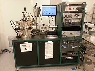
Chemical vapor deposition (CVD) is a vacuum deposition method used to produce high-quality, and high-performance, solid materials. The process is often used in the semiconductor industry to produce thin films.

MEMS is the technology of microscopic devices incorporating both electronic and moving parts. MEMS are made up of components between 1 and 100 micrometres in size, and MEMS devices generally range in size from 20 micrometres to a millimetre, although components arranged in arrays can be more than 1000 mm2. They usually consist of a central unit that processes data and several components that interact with the surroundings.
In physics, sputtering is a phenomenon in which microscopic particles of a solid material are ejected from its surface, after the material is itself bombarded by energetic particles of a plasma or gas. It occurs naturally in outer space, and can be an unwelcome source of wear in precision components. However, the fact that it can be made to act on extremely fine layers of material is utilised in science and industry—there, it is used to perform precise etching, carry out analytical techniques, and deposit thin film layers in the manufacture of optical coatings, semiconductor devices and nanotechnology products. It is a physical vapor deposition technique.

A corona discharge is an electrical discharge caused by the ionization of a fluid such as air surrounding a conductor carrying a high voltage. It represents a local region where the air has undergone electrical breakdown and become conductive, allowing charge to continuously leak off the conductor into the air. A corona discharge occurs at locations where the strength of the electric field around a conductor exceeds the dielectric strength of the air. It is often seen as a bluish glow in the air adjacent to pointed metal conductors carrying high voltages, and emits light by the same mechanism as a gas discharge lamp. Corona discharges can also happen in weather, such as thunderstorms, where objects like ship masts or airplane wings have a charge significantly different from the air around them.
Electrodeless plasma excitation methods include helicon plasma sources, inductively coupled plasmas, and surface-wave-sustained discharges.

A gas-filled tube, also commonly known as a discharge tube or formerly as a Plücker tube, is an arrangement of electrodes in a gas within an insulating, temperature-resistant envelope. Gas-filled tubes exploit phenomena related to electric discharge in gases, and operate by ionizing the gas with an applied voltage sufficient to cause electrical conduction by the underlying phenomena of the Townsend discharge. A gas-discharge lamp is an electric light using a gas-filled tube; these include fluorescent lamps, metal-halide lamps, sodium-vapor lamps, and neon lights. Specialized gas-filled tubes such as krytrons, thyratrons, and ignitrons are used as switching devices in electric devices.

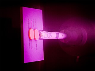
A glow discharge is a plasma formed by the passage of electric current through a gas. It is often created by applying a voltage between two electrodes in a glass tube containing a low-pressure gas. When the voltage exceeds a value called the striking voltage, the gas ionization becomes self-sustaining, and the tube glows with a colored light. The color depends on the gas used.
A thin film is a layer of material ranging from fractions of a nanometer (monolayer) to several micrometers in thickness. The controlled synthesis of materials as thin films is a fundamental step in many applications. A familiar example is the household mirror, which typically has a thin metal coating on the back of a sheet of glass to form a reflective interface. The process of silvering was once commonly used to produce mirrors, while more recently the metal layer is deposited using techniques such as sputtering. Advances in thin film deposition techniques during the 20th century have enabled a wide range of technological breakthroughs in areas such as magnetic recording media, electronic semiconductor devices, integrated passive devices, LEDs, optical coatings, hard coatings on cutting tools, and for both energy generation and storage. It is also being applied to pharmaceuticals, via thin-film drug delivery. A stack of thin films is called a multilayer.
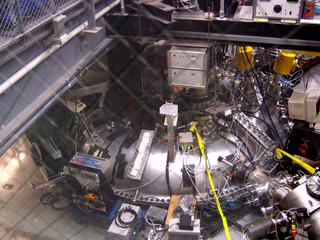
The Madison Symmetric Torus (MST) is a reversed field pinch (RFP) physics experiment with applications to both fusion energy research and astrophysical plasmas.
A capacitively coupled plasma (CCP) is one of the most common types of industrial plasma sources. It essentially consists of two metal electrodes separated by a small distance, placed in a reactor. The gas pressure in the reactor can be lower than atmosphere or it can be atmospheric.
Plasma etching is a form of plasma processing used to fabricate integrated circuits. It involves a high-speed stream of glow discharge (plasma) of an appropriate gas mixture being shot at a sample. The plasma source, known as etch species, can be either charged (ions) or neutral. During the process, the plasma generates volatile etch products at room temperature from the chemical reactions between the elements of the material etched and the reactive species generated by the plasma. Eventually the atoms of the shot element embed themselves at or just below the surface of the target, thus modifying the physical properties of the target.
Physical vapor deposition (PVD), sometimes called physical vapor transport (PVT), describes a variety of vacuum deposition methods which can be used to produce thin films and coatings on substrates including metals, ceramics, glass, and polymers. PVD is characterized by a process in which the material transitions from a condensed phase to a vapor phase and then back to a thin film condensed phase. The most common PVD processes are sputtering and evaporation. PVD is used in the manufacturing of items which require thin films for optical, mechanical, electrical, acoustic or chemical functions. Examples include semiconductor devices such as thin-film solar cells, microelectromechanical devices such as thin film bulk acoustic resonator, aluminized PET film for food packaging and balloons, and titanium nitride coated cutting tools for metalworking. Besides PVD tools for fabrication, special smaller tools used mainly for scientific purposes have been developed.
Plasma activation is a method of surface modification employing plasma processing, which improves surface adhesion properties of many materials including metals, glass, ceramics, a broad range of polymers and textiles and even natural materials such as wood and seeds. Plasma functionalization also refers to the introduction of functional groups on the surface of exposed materials. It is widely used in industrial processes to prepare surfaces for bonding, gluing, coating and painting. Plasma processing achieves this effect through a combination of reduction of metal oxides, ultra-fine surface cleaning from organic contaminants, modification of the surface topography and deposition of functional chemical groups. Importantly, the plasma activation can be performed at atmospheric pressure using air or typical industrial gases including hydrogen, nitrogen and oxygen. Thus, the surface functionalization is achieved without expensive vacuum equipment or wet chemistry, which positively affects its costs, safety and environmental impact. Fast processing speeds further facilitate numerous industrial applications.

Sputter deposition is a physical vapor deposition (PVD) method of thin film deposition by the phenomenon of sputtering. This involves ejecting material from a "target" that is a source onto a "substrate" such as a silicon wafer. Resputtering is re-emission of the deposited material during the deposition process by ion or atom bombardment. Sputtered atoms ejected from the target have a wide energy distribution, typically up to tens of eV. The sputtered ions can ballistically fly from the target in straight lines and impact energetically on the substrates or vacuum chamber. Alternatively, at higher gas pressures, the ions collide with the gas atoms that act as a moderator and move diffusively, reaching the substrates or vacuum chamber wall and condensing after undergoing a random walk. The entire range from high-energy ballistic impact to low-energy thermalized motion is accessible by changing the background gas pressure. The sputtering gas is often an inert gas such as argon. For efficient momentum transfer, the atomic weight of the sputtering gas should be close to the atomic weight of the target, so for sputtering light elements neon is preferable, while for heavy elements krypton or xenon are used. Reactive gases can also be used to sputter compounds. The compound can be formed on the target surface, in-flight or on the substrate depending on the process parameters. The availability of many parameters that control sputter deposition make it a complex process, but also allow experts a large degree of control over the growth and microstructure of the film.
High-power impulse magnetron sputtering is a method for physical vapor deposition of thin films which is based on magnetron sputter deposition. HIPIMS utilises extremely high power densities of the order of kW⋅cm−2 in short pulses (impulses) of tens of microseconds at low duty cycle of < 10%. Distinguishing features of HIPIMS are a high degree of ionisation of the sputtered metal and a high rate of molecular gas dissociation which result in high density of deposited films. The ionization and dissociation degree increase according to the peak cathode power. The limit is determined by the transition of the discharge from glow to arc phase. The peak power and the duty cycle are selected so as to maintain an average cathode power similar to conventional sputtering (1–10 W⋅cm−2).
A microplasma is a plasma of small dimensions, ranging from tens to thousands of micrometers. Microplasmas can be generated at a variety of temperatures and pressures, existing as either thermal or non-thermal plasmas. Non-thermal microplasmas that can maintain their state at standard temperatures and pressures are readily available and accessible to scientists as they can be easily sustained and manipulated under standard conditions. Therefore, they can be employed for commercial, industrial, and medical applications, giving rise to the evolving field of microplasmas.

Plasma is one of four fundamental states of matter, characterized by the presence of a significant portion of charged particles in any combination of ions or electrons. It is the most abundant form of ordinary matter in the universe, mostly in stars, but also dominating the rarefied intracluster medium and intergalactic medium. Plasma can be artificially generated, for example, by heating a neutral gas or subjecting it to a strong electromagnetic field.
Plasma polymerization uses plasma sources to generate a gas discharge that provides energy to activate or fragment gaseous or liquid monomer, often containing a vinyl group, in order to initiate polymerization. Polymers formed from this technique are generally highly branched and highly cross-linked, and adhere to solid surfaces well. The biggest advantage to this process is that polymers can be directly attached to a desired surface while the chains are growing, which reduces steps necessary for other coating processes such as grafting. This is very useful for pinhole-free coatings of 100 picometers to 1-micrometer thickness with solvent insoluble polymers.
An excimer lamp is a source of ultraviolet light based on spontaneous emission of excimer (exciplex) molecules.

Low-energy plasma-enhanced chemical vapor deposition (LEPECVD) is a plasma-enhanced chemical vapor deposition technique used for the epitaxial deposition of thin semiconductor films. A remote low energy, high density DC argon plasma is employed to efficiently decompose the gas phase precursors while leaving the epitaxial layer undamaged, resulting in high quality epilayers and high deposition rates.


