An electric current is a flow of charged particles, such as electrons or ions, moving through an electrical conductor or space. It is defined as the net rate of flow of electric charge through a surface. The moving particles are called charge carriers, which may be one of several types of particles, depending on the conductor. In electric circuits the charge carriers are often electrons moving through a wire. In semiconductors they can be electrons or holes. In an electrolyte the charge carriers are ions, while in plasma, an ionized gas, they are ions and electrons.
A semiconductor is a material that has an electrical conductivity value falling between that of a conductor, such as copper, and an insulator, such as glass. Its resistivity generally falls as its temperature rises; metals behave in the opposite way. In many cases their conducting properties may be altered in useful ways by introducing impurities ("doping") into the crystal structure. When two differently doped regions exist in the same crystal, a semiconductor junction is created. The behavior of charge carriers, which include electrons, ions, and electron holes, at these junctions is the basis of diodes, transistors, and most modern electronics. Some examples of semiconductors are silicon, germanium, gallium arsenide, and elements near the so-called "metalloid staircase" on the periodic table. After silicon, gallium arsenide is the second-most common semiconductor and is used in laser diodes, solar cells, microwave-frequency integrated circuits, and others. Silicon is a critical element for fabricating most electronic circuits.
Electrical resistivity is a fundamental specific property of a material that measures its electrical resistance or how strongly it resists electric current. A low resistivity indicates a material that readily allows electric current. Resistivity is commonly represented by the Greek letter ρ (rho). The SI unit of electrical resistivity is the ohm-metre (Ω⋅m). For example, if a 1 m3 solid cube of material has sheet contacts on two opposite faces, and the resistance between these contacts is 1 Ω, then the resistivity of the material is 1 Ω⋅m.
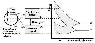
In solid-state physics and solid-state chemistry, a band gap, also called a bandgap or energy gap, is an energy range in a solid where no electronic states exist. In graphs of the electronic band structure of solids, the band gap refers to the energy difference between the top of the valence band and the bottom of the conduction band in insulators and semiconductors. It is the energy required to promote an electron from the valence band to the conduction band. The resulting conduction-band electron are free to move within the crystal lattice and serve as charge carriers to conduct electric current. It is closely related to the HOMO/LUMO gap in chemistry. If the valence band is completely full and the conduction band is completely empty, then electrons cannot move within the solid because there are no available states. If the electrons are not free to move within the crystal lattice, then there is no generated current due to no net charge carrier mobility. However, if some electrons transfer from the valence band to the conduction band, then current can flow. Therefore, the band gap is a major factor determining the electrical conductivity of a solid. Substances having large band gaps are generally insulators, those with small band gaps are semiconductor, and conductors either have very small band gaps or none, because the valence and conduction bands overlap to form a continuous band.

In physics, chemistry, and electronic engineering, an electron hole is a quasiparticle denoting the lack of an electron at a position where one could exist in an atom or atomic lattice. Since in a normal atom or crystal lattice the negative charge of the electrons is balanced by the positive charge of the atomic nuclei, the absence of an electron leaves a net positive charge at the hole's location.

The Fermi level of a solid-state body is the thermodynamic work required to add one electron to the body. It is a thermodynamic quantity usually denoted by μ or EF for brevity. The Fermi level does not include the work required to remove the electron from wherever it came from. A precise understanding of the Fermi level—how it relates to electronic band structure in determining electronic properties; how it relates to the voltage and flow of charge in an electronic circuit—is essential to an understanding of solid-state physics.
In physics, a charge carrier is a particle or quasiparticle that is free to move, carrying an electric charge, especially the particles that carry electric charges in electrical conductors. Examples are electrons, ions and holes. The term is used most commonly in solid state physics. In a conducting medium, an electric field can exert force on these free particles, causing a net motion of the particles through the medium; this is what constitutes an electric current. The electron and the proton are the elementary charge carriers, each carrying one elementary charge (e), of the same magnitude and opposite sign.
In solid-state physics, the electronic band structure of a solid describes the range of energy levels that electrons may have within it, as well as the ranges of energy that they may not have.

In semiconductor production, doping is the intentional introduction of impurities into an intrinsic (undoped) semiconductor for the purpose of modulating its electrical, optical and structural properties. The doped material is referred to as an extrinsic semiconductor.
In solid-state physics, the free electron model is a quantum mechanical model for the behaviour of charge carriers in a metallic solid. It was developed in 1927, principally by Arnold Sommerfeld, who combined the classical Drude model with quantum mechanical Fermi–Dirac statistics and hence it is also known as the Drude–Sommerfeld model.
Organic semiconductors are solids whose building blocks are pi-bonded molecules or polymers made up by carbon and hydrogen atoms and – at times – heteroatoms such as nitrogen, sulfur and oxygen. They exist in the form of molecular crystals or amorphous thin films. In general, they are electrical insulators, but become semiconducting when charges are either injected from appropriate electrodes, upon doping or by photoexcitation.
An intrinsic semiconductor, also called a pure semiconductor, undoped semiconductor or i-type semiconductor, is a semiconductor without any significant dopant species present. The number of charge carriers is therefore determined by the properties of the material itself instead of the amount of impurities. In intrinsic semiconductors the number of excited electrons and the number of holes are equal: n = p. This may be the case even after doping the semiconductor, though only if it is doped with both donors and acceptors equally. In this case, n = p still holds, and the semiconductor remains intrinsic, though doped. This means that some conductors are both intrinsic as well as extrinsic but only if n is equal to p.

Mott insulators are a class of materials that are expected to conduct electricity according to conventional band theories, but turn out to be insulators. These insulators fail to be correctly described by band theories of solids due to their strong electron–electron interactions, which are not considered in conventional band theory. A Mott transition is a transition from a metal to an insulator, driven by the strong interactions between electrons. One of the simplest models that can capture Mott transition is the Hubbard model.
Charge carrier density, also known as carrier concentration, denotes the number of charge carriers per volume. In SI units, it is measured in m−3. As with any density, in principle it can depend on position. However, usually carrier concentration is given as a single number, and represents the average carrier density over the whole material.
An extrinsic semiconductor is one that has been doped; during manufacture of the semiconductor crystal a trace element or chemical called a doping agent has been incorporated chemically into the crystal, for the purpose of giving it different electrical properties than the pure semiconductor crystal, which is called an intrinsic semiconductor. In an extrinsic semiconductor it is these foreign dopant atoms in the crystal lattice that mainly provide the charge carriers which carry electric current through the crystal. The doping agents used are of two types, resulting in two types of extrinsic semiconductor. An electron donor dopant is an atom which, when incorporated in the crystal, releases a mobile conduction electron into the crystal lattice. An extrinsic semiconductor that has been doped with electron donor atoms is called an n-type semiconductor, because the majority of charge carriers in the crystal are negative electrons. An electron acceptor dopant is an atom which accepts an electron from the lattice, creating a vacancy where an electron should be called a hole which can move through the crystal like a positively charged particle. An extrinsic semiconductor which has been doped with electron acceptor atoms is called a p-type semiconductor, because the majority of charge carriers in the crystal are positive holes.

In semiconductor physics, the band gap of a semiconductor can be of two basic types, a direct band gap or an indirect band gap. The minimal-energy state in the conduction band and the maximal-energy state in the valence band are each characterized by a certain crystal momentum (k-vector) in the Brillouin zone. If the k-vectors are different, the material has an "indirect gap". The band gap is called "direct" if the crystal momentum of electrons and holes is the same in both the conduction band and the valence band; an electron can directly emit a photon. In an "indirect" gap, a photon cannot be emitted because the electron must pass through an intermediate state and transfer momentum to the crystal lattice.

In physics, the field effect refers to the modulation of the electrical conductivity of a material by the application of an external electric field.
In solid-state physics, the valence band and conduction band are the bands closest to the Fermi level, and thus determine the electrical conductivity of the solid. In nonmetals, the valence band is the highest range of electron energies in which electrons are normally present at absolute zero temperature, while the conduction band is the lowest range of vacant electronic states. On a graph of the electronic band structure of a semiconducting material, the valence band is located below the Fermi level, while the conduction band is located above it.
Bismuth antimonides, Bismuth-antimonys, or Bismuth-antimony alloys, (Bi1−xSbx) are binary alloys of bismuth and antimony in various ratios.
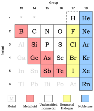
Nonmetals show more variability in their properties than do metals. Metalloids are included here since they behave predominately as chemically weak nonmetals.