
Semiconductor device fabrication is the process used to manufacture semiconductor devices, typically integrated circuits (ICs) such as computer processors, microcontrollers, and memory chips that are present in everyday electronic devices. It is a multiple-step photolithographic and physio-chemical process during which electronic circuits are gradually created on a wafer, typically made of pure single-crystal semiconducting material. Silicon is almost always used, but various compound semiconductors are used for specialized applications.

In electronics, a wafer is a thin slice of semiconductor, such as a crystalline silicon (c-Si), used for the fabrication of integrated circuits and, in photovoltaics, to manufacture solar cells.

STMicroelectronics N.V. is a multinational corporation and technology company of French-Italian origin. It is headquartered in Plan-les-Ouates and listed on the New York Stock Exchange, on the Euronext Paris in Paris and on the Borsa Italiana in Milan. ST is the largest European semiconductor contract manufacturing and design company. The company resulted from the merger of two government-owned semiconductor companies in 1987: Thomson Semiconducteurs of France and SGS Microelettronica of Italy.

Epitaxy refers to a type of crystal growth or material deposition in which new crystalline layers are formed with one or more well-defined orientations with respect to the crystalline seed layer. The deposited crystalline film is called an epitaxial film or epitaxial layer. The relative orientation(s) of the epitaxial layer to the seed layer is defined in terms of the orientation of the crystal lattice of each material. For most epitaxial growths, the new layer is usually crystalline and each crystallographic domain of the overlayer must have a well-defined orientation relative to the substrate crystal structure. Epitaxy can involve single-crystal structures, although grain-to-grain epitaxy has been observed in granular films. For most technological applications, single-domain epitaxy, which is the growth of an overlayer crystal with one well-defined orientation with respect to the substrate crystal, is preferred. Epitaxy can also play an important role while growing superlattice structures.
Applied Materials, Inc. is an American corporation that supplies equipment, services and software for the manufacture of semiconductor chips for electronics, flat panel displays for computers, smartphones, televisions, and solar products. The company also supplies equipment to produce coatings for flexible electronics, packaging and other applications. The company is headquartered in Santa Clara, California, and is the largest supplier of semiconductor equipment in the world based on revenue.
In semiconductor manufacturing, silicon on insulator (SOI) technology is fabrication of silicon semiconductor devices in a layered silicon–insulator–silicon substrate, to reduce parasitic capacitance within the device, thereby improving performance. SOI-based devices differ from conventional silicon-built devices in that the silicon junction is above an electrical insulator, typically silicon dioxide or sapphire. The choice of insulator depends largely on intended application, with sapphire being used for high-performance radio frequency (RF) and radiation-sensitive applications, and silicon dioxide for diminished short-channel effects in other microelectronics devices. The insulating layer and topmost silicon layer also vary widely with application.
An epitaxial wafer is a wafer of semiconducting material made by epitaxial growth (epitaxy) for use in photonics, microelectronics, spintronics, or photovoltaics. The epi layer may be the same material as the substrate, typically monocrystaline silicon, or it may be a silicon dioxide (SoI) or a more exotic material with specific desirable qualities. The purpose of epitaxy is to perfect the crystal structure over the bare substrate below and improve the wafer surface's electrical characteristics, making it suitable for highly complex microprocessors and memory devices.

A solar cell or photovoltaic cell is an electronic device that converts the energy of light directly into electricity by means of the photovoltaic effect. It is a form of photoelectric cell, a device whose electrical characteristics vary when it is exposed to light. Individual solar cell devices are often the electrical building blocks of photovoltaic modules, known colloquially as "solar panels". The common single-junction silicon solar cell can produce a maximum open-circuit voltage of approximately 0.5 to 0.6 volts.
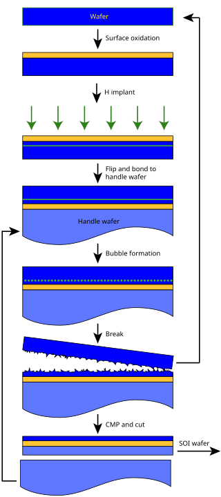
Smart cut is a technological process that enables the transfer of very fine layers of crystalline silicon material onto a mechanical support. It was invented by Michel Bruel of CEA-Leti, and was protected by US patent 5374564. The application of this technological procedure is mainly in the production of silicon-on-insulator (SOI) wafer substrates.
ASM is a Dutch headquartered multinational corporation that specializes in the design, manufacturing, sales and service of semiconductor wafer processing equipment for the fabrication of semiconductor devices. ASM's products are used by semiconductor manufacturers in front-end wafer processing in their semiconductor fabrication plants. ASM's technologies include atomic layer deposition, epitaxy, chemical vapor deposition and diffusion.
SunEdison, Inc. is a renewable energy company headquartered in the U.S. In addition to developing, building, owning, and operating solar power plants and wind energy plants, it also manufactures high purity polysilicon, monocrystalline silicon ingots, silicon wafers, solar modules, solar energy systems, and solar module racking systems. Originally a silicon-wafer manufacturer established in 1959 as the Monsanto Electronic Materials Company, the company was sold by Monsanto in 1989.

Veeco is a global capital equipment supplier, headquartered in the U.S., that designs and builds processing systems used in semiconductor and compound semiconductor manufacturing, data storage and scientific markets for applications such as advanced packaging, photonics, power electronics and display technologies.
GlobalFoundries Inc. (GF) is a multinational semiconductor contract manufacturing and design company incorporated in the Cayman Islands and headquartered in Malta, New York. Created by the divestiture of the manufacturing arm of AMD, the company was privately owned by Mubadala Investment Company, a sovereign wealth fund of the United Arab Emirates, until an initial public offering (IPO) in October 2021.
IQE PLC is a British semiconductor company founded 1988 in Cardiff, Wales, which manufactures advanced epitaxial wafers for a wide range of technology applications for wireless, optoelectronic, electronic and solar devices. IQE specialises in advanced silicon and compound semiconductor materials based on gallium arsenide (GaAs), indium phosphide (InP), gallium nitride (GaN) and silicon. The company is the largest independent outsource producer of epiwafers manufactured by metalorganic vapour phase epitaxy (MOCVD), molecular beam epitaxy (MBE) and chemical vapor deposition (CVD).
Dolphin Design is a semiconductor design company, founded in 2018 following its acquisition by Soitec. Formerly known as Dolphin Integration, it is based in Meylan in the Grenoble region.
There are currently many research groups active in the field of photovoltaics in universities and research institutions around the world. This research can be categorized into three areas: making current technology solar cells cheaper and/or more efficient to effectively compete with other energy sources; developing new technologies based on new solar cell architectural designs; and developing new materials to serve as more efficient energy converters from light energy into electric current or light absorbers and charge carriers.

CEA-Leti is a research institute for electronics and information technologies, based in Grenoble, France. It is one of the world's largest organizations for applied research in microelectronics and nanotechnology. It is part of the French Alternative Energies and Atomic Energy Commission (CEA).

Tower Semiconductor Ltd. is an Israeli company that manufactures integrated circuits using specialty process technologies, including SiGe, BiCMOS, Silicon Photonics, SOI, mixed-signal and RFCMOS, CMOS image sensors, non-imaging sensors, power management (BCD), and non-volatile memory (NVM) as well as MEMS capabilities. Tower Semiconductor also owns 51% of TPSCo, an enterprise with Nuvoton Technology Corporation Japan (NTCJ).
The Fraunhofer Institute for Solar Energy Systems ISE is an institute of the Fraunhofer-Gesellschaft. Located in Freiburg, Germany, The Institute performs applied scientific and engineering research and development for all areas of solar energy. Fraunhofer ISE has three external branches in Germany which carry out work on solar cell and semiconductor material development: the Laboratory and Service Center (LSC) in Gelsenkirchen, the Technology Center of Semiconductor Materials (THM) in Freiberg, and the Fraunhofer Center for Silicon Photovoltaics (CSP) in Halle. From 2006 to 2016 Eicke Weber was the director of Fraunhofer ISE. With over 1,100 employees, Fraunhofer ISE is the largest institute for applied solar energy research in Europe. The 2012 Operational Budget including investments was 74.3 million euro.
Weebit Nano is a public semiconductor IP company founded in Israel in 2015 and headquartered in Hod Hasharon, Israel. The company develops Resistive Random-Access Memory technologies. Resistive Random-Access Memory is a specialized form of non-volatile memory (NVM) for the semiconductor industry. The company’s products are targeted at a broad range of NVM markets where persistence, performance, and endurance are all required. ReRAM technology can be integrated in electronic devices like wearables, Internet of Things (IoT) endpoints, smartphones, robotics, autonomous vehicles, and 5G cellular communications, among other products. Weebit Nano’s IP can be licensed to semiconductor companies and semiconductor fabs.