Electronics is a scientific and engineering discipline that studies and applies the principles of physics to design, create, and operate devices that manipulate electrons and other electrically charged particles. Electronics is a subfield of electrical engineering, but it differs from it in that it focuses on using active devices such as transistors, diodes, and integrated circuits to control and amplify the flow of electric current and to convert it from one form to another, such as from alternating current (AC) to direct current (DC) or from analog signals to digital signals. Electronics also encompasses the fields of microelectronics, nanoelectronics, optoelectronics, and quantum electronics, which deal with the fabrication and application of electronic devices at microscopic, nanoscopic, optical, and quantum scales.
A semiconductor is a material that has an electrical conductivity value falling between that of a conductor, such as copper, and an insulator, such as glass. Its resistivity generally falls as its temperature rises; metals behave in the opposite way. In many cases their conducting properties may be altered in useful ways by introducing impurities ("doping") into the crystal structure. When two differently doped regions exist in the same crystal, a semiconductor junction is created. The behavior of charge carriers, which include electrons, ions, and electron holes, at these junctions is the basis of diodes, transistors, and most modern electronics. Some examples of semiconductors are silicon, germanium, gallium arsenide, and elements near the so-called "metalloid staircase" on the periodic table. After silicon, gallium arsenide is the second-most common semiconductor and is used in laser diodes, solar cells, microwave-frequency integrated circuits, and others. Silicon is a critical element for fabricating most electronic circuits.

Photonics is a branch of optics that involves the application of generation, detection, and manipulation of light in form of photons through emission, transmission, modulation, signal processing, switching, amplification, and sensing. Photonics is closely related to quantum electronics, where quantum electronics deals with the theoretical part of it while photonics deal with its engineering applications. Though covering all light's technical applications over the whole spectrum, most photonic applications are in the range of visible and near-infrared light. The term photonics developed as an outgrowth of the first practical semiconductor light emitters invented in the early 1960s and optical fibers developed in the 1970s.

A thermographic camera is a device that creates an image using infrared (IR) radiation, similar to a normal camera that forms an image using visible light. Instead of the 400–700 nanometre (nm) range of the visible light camera, infrared cameras are sensitive to wavelengths from about 1,000 nm to about 14,000 nm (14 μm). The practice of capturing and analyzing the data they provide is called thermography.
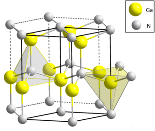
Gallium nitride is a binary III/V direct bandgap semiconductor commonly used in blue light-emitting diodes since the 1990s. The compound is a very hard material that has a Wurtzite crystal structure. Its wide band gap of 3.4 eV affords it special properties for applications in optoelectronic, high-power and high-frequency devices. For example, GaN is the substrate which makes violet (405 nm) laser diodes possible, without requiring nonlinear optical frequency-doubling.

Electromigration is the transport of material caused by the gradual movement of the ions in a conductor due to the momentum transfer between conducting electrons and diffusing metal atoms. The effect is important in applications where high direct current densities are used, such as in microelectronics and related structures. As the structure size in electronics such as integrated circuits (ICs) decreases, the practical significance of this effect increases.

Oleg Vladimirovich Losev was a Russian scientist and inventor who made significant discoveries in the field of semiconductor junctions and the light emitting diode (LED).
Sir Christopher Maxwell Snowden, is a British electronic engineer and academic. He was the former Vice-Chancellor of Surrey University (2005–2015), and of the University of Southampton (2015–2019). He was president of Universities UK for a two-year term until 31 July 2015. He is currently the chairman of the ERA Foundation.
David Keane Ferry is the Regents' Professor of Electrical Engineering at Arizona State University (ASU), notable for his research in semiconductor devices.
Alexander Rudolf Hamilton is with the School of Physics at the University of New South Wales (UNSW). He is notable in the area of experimental condensed matter physics, particularly semiconductor nanofabrication and the study of quantum effects in nanometer scale electronic devices at ultra-low temperatures.
Crosslight Software Inc. is an international company headquartered in greater Vancouver, British Columbia, Canada. Officially spun off from the National Research Council of Canada (NRC) in 1995, it provides Technology Computer Aided Design (TCAD) tools for semiconductor device and process simulations.

Alexander A. Balandin is an electrical engineer, solid-state physicist, and materials scientist best known for the experimental discovery of unique thermal properties of graphene and their theoretical explanation; studies of phonons in nanostructures and low-dimensional materials, which led to the development of the field of phonon engineering; investigation of low-frequency electronic noise in materials and devices; and demonstration of the first charge-density-wave quantum devices operating at room temperature.
The following outline is provided as an overview of and topical guide to electronics:
The index of physics articles is split into multiple pages due to its size.
Mohamed M. Atalla was an Egyptian-American engineer, physicist, cryptographer, inventor and entrepreneur. He was a semiconductor pioneer who made important contributions to modern electronics. He is best known for inventing the MOSFET in 1959, which along with Atalla's earlier surface passivation processes, had a significant impact on the development of the electronics industry. He is also known as the founder of the data security company Atalla Corporation, founded in 1972. He received the Stuart Ballantine Medal and was inducted into the National Inventors Hall of Fame for his important contributions to semiconductor technology as well as data security.
Active thermography is an advanced nondestructive testing procedure, which uses a thermography measurement of a tested material thermal response after its external excitation. This principle can be used also for non-contact infrared non-destructive testing (IRNDT) of materials.
Elias Burstein was an American experimental condensed matter physicist whose active career in science spanned seven decades. He is known for his pioneering fundamental research in the optical physics of solids; for writing and editing hundreds of articles and other publications; for bringing together scientists from around the world in international meetings, conferences, and symposia; and for training and mentoring dozens of younger physicists.
Roger John Malik is a physicist, engineer and inventor.
Martin Kuball is the chair of the Royal Academy of Engineering in Emerging Technologies, professor in physics at the University of Bristol, United Kingdom, and director of the Centre for Device Thermography and Reliability (CDTR).

Aristos Christou is an American engineer and scientist, academic professor and researcher. He is a Professor of Materials Science, Professor of Mechanical Engineering and Professor of Reliability Engineering at the University of Maryland.