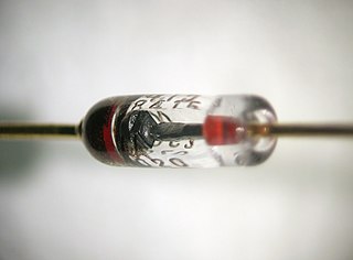
A diode is a two-terminal electronic component that conducts current primarily in one direction. It has low resistance in one direction and high resistance in the other.
A PIN diode is a diode with a wide, undoped intrinsic semiconductor region between a p-type semiconductor and an n-type semiconductor region. The p-type and n-type regions are typically heavily doped because they are used for ohmic contacts.

The Schottky diode, also known as Schottky barrier diode or hot-carrier diode, is a semiconductor diode formed by the junction of a semiconductor with a metal. It has a low forward voltage drop and a very fast switching action. The cat's-whisker detectors used in the early days of wireless and metal rectifiers used in early power applications can be considered primitive Schottky diodes.

In electronics, a varicap diode, varactor diode, variable capacitance diode, variable reactance diode or tuning diode is a type of diode designed to exploit the voltage-dependent capacitance of a reverse-biased p–n junction.
An avalanche photodiode (APD) is a highly sensitive type of photodiode, which in general are semiconductor diodes that exploit the photoelectric effect to convert light into electricity. APDs use materials and a structure optimised for operating with high reverse bias, approaching the reverse breakdown voltage, such that charge carriers generated by the photoelectric effect are multiplied by an avalanche breakdown; thus they can be used to detect relatively small amounts of light.

A Schottky barrier, named after Walter H. Schottky, is a potential energy barrier for electrons formed at a metal–semiconductor junction. Schottky barriers have rectifying characteristics, suitable for use as a diode. One of the primary characteristics of a Schottky barrier is the Schottky barrier height, denoted by ΦB. The value of ΦB depends on the combination of metal and semiconductor.

A tunnel diode or Esaki diode is a type of semiconductor diode that has effectively "negative resistance" due to the quantum mechanical effect called tunneling. It was invented in August 1957 by Leo Esaki when working at Tokyo Tsushin Kogyo, now known as Sony. In 1973, Esaki received the Nobel Prize in Physics for experimental demonstration of the electron tunneling effect in semiconductors. Robert Noyce independently devised the idea of a tunnel diode while working for William Shockley, but was discouraged from pursuing it. Tunnel diodes were first manufactured by Sony in 1957, followed by General Electric and other companies from about 1960, and are still made in low volume today.

A p–n junction is a combination of two types of semiconductor materials, p-type and n-type, in a single crystal. The "n" (negative) side contains freely-moving electrons, while the "p" (positive) side contains freely-moving electron holes. Connecting the two materials causes creation of a depletion region near the boundary, as the free electrons fill the available holes, which in turn allows electric current to pass through the junction only in one direction.
A MESFET is a field-effect transistor semiconductor device similar to a JFET with a Schottky (metal–semiconductor) junction instead of a p–n junction for a gate.
In electronics, a frequency multiplier is an electronic circuit that generates an output signal and that output frequency is a harmonic (multiple) of its input frequency. Frequency multipliers consist of a nonlinear circuit that distorts the input signal and consequently generates harmonics of the input signal. A subsequent bandpass filter selects the desired harmonic frequency and removes the unwanted fundamental and other harmonics from the output.
An IMPATT diode is a form of high-power semiconductor diode used in high-frequency microwave electronics devices. They have negative resistance and are used as oscillators and amplifiers at microwave frequencies. They operate at frequencies of about 3 and 100 GHz, or higher. The main advantage is their high-power capability; single IMPATT diodes can produce continuous microwave outputs of up to 3 kilowatts, and pulsed outputs of much higher power. These diodes are used in a variety of applications from low-power radar systems to proximity alarms. A major drawback of IMPATT diodes is the high level of phase noise they generate. This results from the statistical nature of the avalanche process.

A Gunn diode, also known as a transferred electron device (TED), is a form of diode, a two-terminal semiconductor electronic component, with negative differential resistance, used in high-frequency electronics. It is based on the "Gunn effect" discovered in 1962 by physicist J. B. Gunn. Its main uses are in electronic oscillators to generate microwaves, in applications such as radar speed guns, microwave relay data link transmitters, and automatic door openers.
Deep-level transient spectroscopy (DLTS) is an experimental tool for studying electrically active defects in semiconductors. DLTS establishes fundamental defect parameters and measures their concentration in the material. Some of the parameters are considered as defect "finger prints" used for their identifications and analysis.
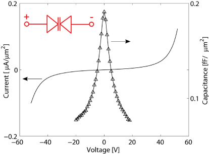
Capacitance–voltage profiling is a technique for characterizing semiconductor materials and devices. The applied voltage is varied, and the capacitance is measured and plotted as a function of voltage. The technique uses a metal–semiconductor junction or a p–n junction or a MOSFET to create a depletion region, a region which is empty of conducting electrons and holes, but may contain ionized donors and electrically active defects or traps. The depletion region with its ionized charges inside behaves like a capacitor. By varying the voltage applied to the junction it is possible to vary the depletion width. The dependence of the depletion width upon the applied voltage provides information on the semiconductor's internal characteristics, such as its doping profile and electrically active defect densities., Measurements may be done at DC, or using both DC and a small-signal AC signal, or using a large-signal transient voltage.

In electronics, a step recovery diode is a semiconductor junction diode with the ability to generate extremely short pulses. It has a variety of uses in microwave electronics as pulse generator or parametric amplifier.
This article provides a more detailed explanation of p–n diode behavior than is found in the articles p–n junction or diode.
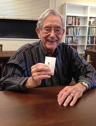
James Robert Biard was an American electrical engineer and inventor who held 73 U.S. patents. Some of his more significant patents include the first infrared light-emitting diode (LED), the optical isolator, Schottky clamped logic circuits, silicon Metal Oxide Semiconductor Read Only Memory, a low bulk leakage current avalanche photodetector, and fiber-optic data links. In 1980, Biard became a member of the staff of Texas A&M University as an Adjunct Professor of Electrical Engineering. In 1991, he was elected as a member into the National Academy of Engineering for contributions to semiconductor light-emitting diodes and lasers, Schotky-clamped logic, and read-only memories.

The field-effect transistor (FET) is a type of transistor that uses an electric field to control the flow of current in a semiconductor. It comes in two types: junction FET (JFET) and metal-oxide-semiconductor FET (MOSFET). FETs have three terminals: source, gate, and drain. FETs control the flow of current by the application of a voltage to the gate, which in turn alters the conductivity between the drain and source.
Metal–insulator–metal (MIM) diode is a type of nonlinear device very similar to a semiconductor diode and capable of very fast operation. Depending on the geometry and the material used for fabrication, the operation mechanisms are governed either by quantum tunnelling or thermal activation.
Geometric diodes, also known as morphological diodes, use the shape of their structure and ballistic / quasi-ballistic electron transport to create diode behavior. Geometric diodes differ from all other forms of diodes because they do not rely on a depletion region or a potential barrier to create their diode behavior. Instead of a potential barrier, an asymmetry in the geometry of the material creates an asymmetry in forward vs reverse bias current.