Related Research Articles

Microelectromechanical systems (MEMS), also written as micro-electro-mechanical systems and the related micromechatronics and microsystems constitute the technology of microscopic devices, particularly those with moving parts. They merge at the nanoscale into nanoelectromechanical systems (NEMS) and nanotechnology. MEMS are also referred to as micromachines in Japan and microsystem technology (MST) in Europe.

A photoresist is a light-sensitive material used in several processes, such as photolithography and photoengraving, to form a patterned coating on a surface. This process is crucial in the electronic industry.

A printed circuit board is a medium used in electrical and electronic engineering to connect electronic components to one another in a controlled manner. It takes the form of a laminated sandwich structure of conductive and insulating layers: each of the conductive layers is designed with an artwork pattern of traces, planes and other features etched from one or more sheet layers of copper laminated onto and/or between sheet layers of a non-conductive substrate. Electrical components may be fixed to conductive pads on the outer layers in the shape designed to accept the component's terminals, generally by means of soldering, to both electrically connect and mechanically fasten them to it. Another manufacturing process adds vias: plated-through holes that allow interconnections between layers.
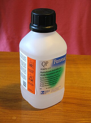
Hydrofluoric acid is a solution of hydrogen fluoride (HF) in water. Solutions of HF are colourless, acidic and highly corrosive. It is used to make most fluorine-containing compounds; examples include the commonly used pharmaceutical antidepressant medication fluoxetine (Prozac) and the material PTFE (Teflon). Elemental fluorine is produced from it. It is commonly used to etch glass and silicon wafers.
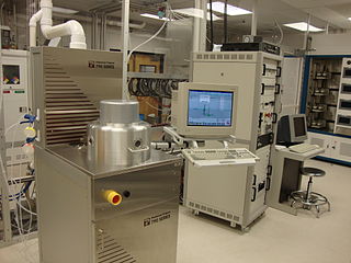
Reactive-ion etching (RIE) is an etching technology used in microfabrication. RIE is a type of dry etching which has different characteristics than wet etching. RIE uses chemically reactive plasma to remove material deposited on wafers. The plasma is generated under low pressure (vacuum) by an electromagnetic field. High-energy ions from the plasma attack the wafer surface and react with it.
Dry etching refers to the removal of material, typically a masked pattern of semiconductor material, by exposing the material to a bombardment of ions that dislodge portions of the material from the exposed surface. A common type of dry etching is reactive-ion etching. Unlike with many of the wet chemical etchants used in wet etching, the dry etching process typically etches directionally or anisotropically.
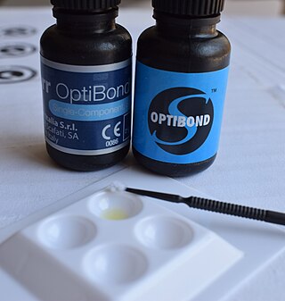
Also known as a "bonderizer" bonding agents are resin materials used to make a dental composite filling material adhere to both dentin and enamel.
Deep reactive-ion etching (DRIE) is a highly anisotropic etch process used to create deep penetration, steep-sided holes and trenches in wafers/substrates, typically with high aspect ratios. It was developed for microelectromechanical systems (MEMS), which require these features, but is also used to excavate trenches for high-density capacitors for DRAM and more recently for creating through silicon vias (TSVs) in advanced 3D wafer level packaging technology. In DRIE, the substrate is placed inside a reactor, and several gases are introduced. A plasma is struck in the gas mixture which breaks the gas molecules into ions. The ions accelerated towards, and react with the surface of the material being etched, forming another gaseous element. This is known as the chemical part of the reactive ion etching. There is also a physical part, if ions have enough energy, they can knock atoms out of the material to be etched without chemical reaction.

Corona treatment is a surface modification technique that uses a low temperature corona discharge plasma to impart changes in the properties of a surface. The corona plasma is generated by the application of high voltage to an electrode that has a sharp tip. The plasma forms at the tip. A linear array of electrodes is often used to create a curtain of corona plasma. Materials such as plastics, cloth, or paper may be passed through the corona plasma curtain in order to change the surface energy of the material. All materials have an inherent surface energy. Surface treatment systems are available for virtually any surface format including dimensional objects, sheets and roll goods that are handled in a web format. Corona treatment is a widely used surface treatment method in the plastic film, extrusion, and converting industries.

Powder coating is a type of coating that is applied as a free-flowing, dry powder. Unlike conventional liquid paint which is delivered via an evaporating solvent, powder coating is typically applied electrostatically and then cured under heat or with ultraviolet light. The powder may be a thermoplastic or a thermoset polymer. It is usually used to create a hard finish that is tougher than conventional paint. Powder coating is mainly used for coating of metals, such as household appliances, aluminium extrusions, drum hardware, automobiles, and bicycle frames. Advancements in powder coating technology like UV curable powder coatings allow for other materials such as plastics, composites, carbon fiber, and MDF to be powder coated due to the minimum heat and oven dwell time required to process these components.
Plasma etching is a form of plasma processing used to fabricate integrated circuits. It involves a high-speed stream of glow discharge (plasma) of an appropriate gas mixture being shot at a sample. The plasma source, known as etch species, can be either charged (ions) or neutral. During the process, the plasma generates volatile etch products at room temperature from the chemical reactions between the elements of the material etched and the reactive species generated by the plasma. Eventually the atoms of the shot element embed themselves at or just below the surface of the target, thus modifying the physical properties of the target.

Plasma cleaning is the removal of impurities and contaminants from surfaces through the use of an energetic plasma or dielectric barrier discharge (DBD) plasma created from gaseous species. Gases such as argon and oxygen, as well as mixtures such as air and hydrogen/nitrogen are used. The plasma is created by using high frequency voltages to ionise the low pressure gas, although atmospheric pressure plasmas are now also common.

Etching is used in microfabrication to chemically remove layers from the surface of a wafer during manufacturing. Etching is a critically important process module, and every wafer undergoes many etching steps before it is complete.
Adhesive bonding describes a wafer bonding technique with applying an intermediate layer to connect substrates of different types of materials. Those connections produced can be soluble or insoluble. The commercially available adhesive can be organic or inorganic and is deposited on one or both substrate surfaces. Adhesives, especially the well-established SU-8, and benzocyclobutene (BCB), are specialized for MEMS or electronic component production.

The Wright etch is a preferential etch for revealing defects in <100>- and <111>-oriented, p- and n-type silicon wafers used for making transistors, microprocessors, memories, and other components. Revealing, identifying, and remedying such defects is essential for progress along the path predicted by Moore's Law. It was developed by Margaret Wright Jenkins (1936-2018) in 1976 while working in research and development at Motorola Inc. in Phoenix, AZ. It was published in 1977. This etchant reveals clearly defined oxidation-induced stacking faults, dislocations, swirls and striations with minimum surface roughness or extraneous pitting. These defects are known causes of shorts and current leakage in finished semiconductor devices should they fall across isolated junctions. A relatively low etch rate at room temperature provides etch control. The long shelf life of this etchant allows the solution to be stored in large quantities.
Plasma-activated bonding is a derivative, directed to lower processing temperatures for direct bonding with hydrophilic surfaces. The main requirements for lowering temperatures of direct bonding are the use of materials melting at low temperatures and with different coefficients of thermal expansion (CTE).

Biomaterials are materials that are used in contact with biological systems. Biocompatibility and applicability of surface modification with current uses of metallic, polymeric and ceramic biomaterials allow alteration of properties to enhance performance in a biological environment while retaining bulk properties of the desired device.
Chemical milling or industrial etching is the subtractive manufacturing process of using baths of temperature-regulated etching chemicals to remove material to create an object with the desired shape. Other names for chemical etching include photo etching, chemical etching, photo chemical etching and photochemical machining. It is mostly used on metals, though other materials are increasingly important. It was developed from armor-decorating and printing etching processes developed during the Renaissance as alternatives to engraving on metal. The process essentially involves bathing the cutting areas in a corrosive chemical known as an etchant, which reacts with the material in the area to be cut and causes the solid material to be dissolved; inert substances known as maskants are used to protect specific areas of the material as resists.
The surface chemistry of paper is responsible for many important paper properties, such as gloss, waterproofing, and printability. Many components are used in the paper-making process that affect the surface.
Titanium adhesive bonding is an engineering process used in the aerospace industry, medical-device manufacture and elsewhere. Titanium alloy is often used in medical and military applications because of its strength, weight, and corrosion resistance characteristics. In implantable medical devices, titanium is used because of its biocompatibility and its passive, stable oxide layer. Also, titanium allergies are rare and in those cases mitigations like Parylene coating are used. In the aerospace industry titanium is often bonded to save cost, touch times, and the need for mechanical fasteners. In the past, Russian submarines' hulls were completely made of titanium because the non-magnetic nature of the material went undetected by the defense technology at that time. Bonding adhesive to titanium requires preparing the surface beforehand, and there is not a single solution for all applications. For example, etchant and chemical methods are not biocompatible and cannot be employed when the device will come into contact with blood and tissue. Mechanical surface roughness techniques like sanding and laser roughening may make the surface brittle and create micro-hardness regions that would not be suitable for cyclic loading found in military applications. Air oxidation at high temperatures will produce a crystalline oxide layer at a lower investment cost, but the increased temperatures can deform precision parts. The type of adhesive, thermosetting or thermoplastic, and curing methods are also factors in titanium bonding because of the adhesive's interaction with the treated oxide layer. Surface treatments can also be combined. For example, a grit blast process can be followed by a chemical etch and a primer application.
References
- 1 2 3 4 5 6 7 8 9 10 11 12 Ebnesajjad, Sina (2015). Fluoroplastics, Vol. 1: Non-Melt Processible Fluoroplastics. United States: Elsevier. pp. 314–335. ISBN 9781455732005.
- ↑ "Bonding PTFE Materials for Microwave Stripline Packages and Other Multilayer Circuits". 2003.
- ↑ "Material Safety Data Sheet, Poly-Etch" (PDF). 2009.
- ↑ "Safety Data Sheet, FluoroEtch Safety Solvent" (PDF). 2016.
- ↑ "Material Safety Data Sheet, Poly-Etch W" (PDF). 2009.
- 1 2 3 4 5 6 7 8 9 10 11 Kim, Sung R. (2000). "Surface Modification of Poly(tetrafluoroethylene) Film by Chemical Etching, Plasma, and Ion Beam Treatments". Journal of Applied Polymer Science. 77 (9): 1913–1920. doi:10.1002/1097-4628(20000829)77:9<1913::aid-app7>3.0.co;2-#.
- 1 2 3 Marchesi, J. T.; Keith, H. D.; Garton, A. (1992). "Adhesion to Sodium Naphthalenide Treated Fluoropolymers. Part III. Mechanism off Adhesion". The Journal of Adhesion. 39 (4): 185–205. doi:10.1080/00218469208030462.
- 1 2 3 4 5 6 7 8 9 10 Badey, J.P.; Espuche, E.; Jugnet, Y.; Chabert, B.; Tran, Minh Duc (1996). "Influence of chemical and plasma treatments on the adhesive properties of PTFE with an epoxy resin". Int. J. Adhesion and Adhesives. 16 (3): 173–178. doi:10.1016/0143-7496(95)00042-9.
- 1 2 3 Brewis, D. M.; Mathieson, I.; Sutherland, I.; Cayless, R. A. (1993). "Adhesion Studies of Fluoropolymers". The Journal of Adhesion. 41 (1–4): 113–128. doi:10.1080/00218469308026557.
- 1 2 3 Kaplan, S. L.; Lopata, E. S.; Smith, Jared (1993). "Plasma Processes and Adhesive Bonding of Polytetrafluoroethylene". Surface and Interface Analysis. 20 (5): 331–336. doi:10.1002/sia.740200502.
- ↑ Rauh, M.; Ihlemann, J.; Koch, A. (2007). "Laser surface roughening of PTFE for increased bonding strength". Applied Physics A: Materials Science & Processing. 88 (2): 231–233. Bibcode:2007ApPhA..88..231R. doi:10.1007/s00339-007-4070-1. S2CID 97747626.