Kelvin probe force microscope

Last updated
In Kelvin probe force microscopy, a conducting cantilever is scanned over a surface at a constant height in order to map the work function of the surface. Kelvin probe force microscopy.svg
In Kelvin probe force microscopy, a conducting cantilever is scanned over a surface at a constant height in order to map the work function of the surface.
A typical scanning Kelvin probe (SKP) instrument. On the left is the control unit with lock-in amplifier and backing potential controller. On the right is the x, y, z scanning axis with vibrator, electrometer and probe mounted. SKP Typical Instrument2.jpg
A typical scanning Kelvin probe (SKP) instrument. On the left is the control unit with lock-in amplifier and backing potential controller. On the right is the x, y, z scanning axis with vibrator, electrometer and probe mounted.

Kelvin probe force microscopy (KPFM), also known as surface potential microscopy, is a noncontact variant of atomic force microscopy (AFM). [1] [2] [3] By raster scanning in the x,y plane the work function of the sample can be locally mapped for correlation with sample features. When there is little or no magnification, this approach can be described as using a scanning Kelvin probe (SKP). These techniques are predominantly used to measure corrosion and coatings.

Contents

With KPFM, the work function of surfaces can be observed at atomic or molecular scales. The work function relates to many surface phenomena, including catalytic activity, reconstruction of surfaces, doping and band-bending of semiconductors, charge trapping in dielectrics and corrosion. The map of the work function produced by KPFM gives information about the composition and electronic state of the local structures on the surface of a solid.

History

The SKP technique is based on parallel plate capacitor experiments performed by Lord Kelvin in 1898. [4] In the 1930s William Zisman built upon Lord Kelvin's experiments to develop a technique to measure contact potential differences of dissimilar metals. [5]

Working principle

The changes to the Fermi levels of the scanning Kelvin probe (SKP) sample and probe during measurement are shown. On the electrical connection of the probe and sample their Fermi levels equilibrate, and a charge develops at the probe and sample. A backing potential is applied to null this charge, returning the sample Fermi level to its original position. SKP Fermi level diagram.png
The changes to the Fermi levels of the scanning Kelvin probe (SKP) sample and probe during measurement are shown. On the electrical connection of the probe and sample their Fermi levels equilibrate, and a charge develops at the probe and sample. A backing potential is applied to null this charge, returning the sample Fermi level to its original position.

In SKP the probe and sample are held parallel to each other and electrically connected to form a parallel plate capacitor. The probe is selected to be of a different material to the sample, therefore each component initially has a distinct Fermi level. When electrical connection is made between the probe and the sample electron flow can occur between the probe and the sample in the direction of the higher to the lower Fermi level. This electron flow causes the equilibration of the probe and sample Fermi levels. Furthermore, a surface charge develops on the probe and the sample, with a related potential difference known as the contact potential (Vc). In SKP the probe is vibrated along a perpendicular to the plane of the sample. [6] This vibration causes a change in probe to sample distance, which in turn results in the flow of current, taking the form of an ac sine wave. The resulting ac sine wave is demodulated to a dc signal through the use of a lock-in amplifier. [7] Typically the user must select the correct reference phase value used by the lock-in amplifier. Once the dc potential has been determined, an external potential, known as the backing potential (Vb) can be applied to null the charge between the probe and the sample. When the charge is nullified, the Fermi level of the sample returns to its original position. This means that Vb is equal to -Vc, which is the work function difference between the SKP probe and the sample measured. [8]

Simplified illustration of the scanning Kelvin probe (SKP) technique. The probe is shown to vibrate in z, perpendicular to the sample plane. The probe and sample form a parallel plate capacitor as shown. SKP Simplified.jpg
Simplified illustration of the scanning Kelvin probe (SKP) technique. The probe is shown to vibrate in z, perpendicular to the sample plane. The probe and sample form a parallel plate capacitor as shown.
Block diagram of a scanning Kelvin probe (SKP) instrument showing computer, control unit, scan axes, vibrator, probe, and sample Scanning Kelvin Probe (SKP) Block Diagram.jpg
Block diagram of a scanning Kelvin probe (SKP) instrument showing computer, control unit, scan axes, vibrator, probe, and sample

The cantilever in the AFM is a reference electrode that forms a capacitor with the surface, over which it is scanned laterally at a constant separation. The cantilever is not piezoelectrically driven at its mechanical resonance frequency ω0 as in normal AFM although an alternating current (AC) voltage is applied at this frequency.

When there is a direct-current (DC) potential difference between the tip and the surface, the AC+DC voltage offset will cause the cantilever to vibrate. The origin of the force can be understood by considering that the energy of the capacitor formed by the cantilever and the surface is

plus terms at DC. Only the cross-term proportional to the VDC·VAC product is at the resonance frequency ω0. The resulting vibration of the cantilever is detected using usual scanned-probe microscopy methods (typically involving a diode laser and a four-quadrant detector). A null circuit is used to drive the DC potential of the tip to a value which minimizes the vibration. A map of this nulling DC potential versus the lateral position coordinate therefore produces an image of the work function of the surface.

A related technique, electrostatic force microscopy (EFM), directly measures the force produced on a charged tip by the electric field emanating from the surface. EFM operates much like magnetic force microscopy in that the frequency shift or amplitude change of the cantilever oscillation is used to detect the electric field. However, EFM is much more sensitive to topographic artifacts than KPFM. Both EFM and KPFM require the use of conductive cantilevers, typically metal-coated silicon or silicon nitride. Another AFM-based technique for the imaging of electrostatic surface potentials, scanning quantum dot microscopy, [9] quantifies surface potentials based on their ability to gate a tip-attached quantum dot.

Factors affecting SKP measurements

The quality of an SKP measurement is affected by a number of factors. This includes the diameter of the SKP probe, the probe to sample distance, and the material of the SKP probe. The probe diameter is important in the SKP measurement because it affects the overall resolution of the measurement, with smaller probes leading to improved resolution. [10] [11] On the other hand, reducing the size of the probe causes an increase in fringing effects which reduces the sensitivity of the measurement by increasing the measurement of stray capacitances. [10] The material used in the construction of the SKP probe is important to the quality of the SKP measurement. [12] This occurs for a number of reasons. Different materials have different work function values which will affect the contact potential measured. Different materials have different sensitivity to humidity changes. The material can also affect the resulting lateral resolution of the SKP measurement. In commercial probes tungsten is used, [13] though probes of platinum, [14] copper, [15] gold, [16] and NiCr has been used. [17] The probe to sample distance affects the final SKP measurement, with smaller probe to sample distances improving the lateral resolution [11] and the signal-to-noise ratio of the measurement. [18] Furthermore, reducing the SKP probe to sample distance increases the intensity of the measurement, where the intensity of the measurement is proportional to 1/d2, where d is the probe to sample distance. [19] The effects of changing probe to sample distance on the measurement can be counteracted by using SKP in constant distance mode.

Work function

The Kelvin probe force microscope or Kelvin force microscope (KFM) is based on an AFM set-up and the determination of the work function is based on the measurement of the electrostatic forces between the small AFM tip and the sample. The conducting tip and the sample are characterized by (in general) different work functions, which represent the difference between the Fermi level and the vacuum level for each material. If both elements were brought in contact, a net electric current would flow between them until the Fermi levels were aligned. The difference between the work functions is called the contact potential difference and is denoted generally with VCPD. An electrostatic force exists between tip and sample, because of the electric field between them. For the measurement a voltage is applied between tip and sample, consisting of a DC-bias VDC and an AC-voltage VAC sin(ωt) of frequency ω.

Tuning the AC-frequency to the resonant frequency of the AFM cantilever results in an improved sensitivity. The electrostatic force in a capacitor may be found by differentiating the energy function with respect to the separation of the elements and can be written as

where C is the capacitance, z is the separation, and V is the voltage, each between tip and surface. Substituting the previous formula for voltage (V) shows that the electrostatic force can be split up into three contributions, as the total electrostatic force F acting on the tip then has spectral components at the frequencies ω and .

The DC component, FDC, contributes to the topographical signal, the term Fω at the characteristic frequency ω is used to measure the contact potential and the contribution F can be used for capacitance microscopy.

Contact potential measurements

For contact potential measurements a lock-in amplifier is used to detect the cantilever oscillation at ω. During the scan VDC will be adjusted so that the electrostatic forces between the tip and the sample become zero and thus the response at the frequency ω becomes zero. Since the electrostatic force at ω depends on VDC − VCPD, the value of VDC that minimizes the ω-term corresponds to the contact potential. Absolute values of the sample work function can be obtained if the tip is first calibrated against a reference sample of known work function. [20] Apart from this, one can use the normal topographic scan methods at the resonance frequency ω independently of the above. Thus, in one scan, the topography and the contact potential of the sample are determined simultaneously. This can be done in (at least) two different ways: 1) The topography is captured in AC mode which means that the cantilever is driven by a piezo at its resonant frequency. Simultaneously the AC voltage for the KPFM measurement is applied at a frequency slightly lower than the resonant frequency of the cantilever. In this measurement mode the topography and the contact potential difference are captured at the same time and this mode is often called single-pass. 2) One line of the topography is captured either in contact or AC mode and is stored internally. Then, this line is scanned again, while the cantilever remains on a defined distance to the sample without a mechanically driven oscillation but the AC voltage of the KPFM measurement is applied and the contact potential is captured as explained above. It is important to note that the cantilever tip must not be too close to the sample in order to allow good oscillation with applied AC voltage. Therefore, KPFM can be performed simultaneously during AC topography measurements but not during contact topography measurements.

Applications

The Volta potential measured by SKP is directly proportional to the corrosion potential of a material, [21] as such SKP has found widespread use in the study of the fields of corrosion and coatings. In the field of coatings for example, a scratched region of a self-healing shape memory polymer coating containing a heat generating agent on aluminium alloys was measured by SKP. [22] Initially after the scratch was made the Volta potential was noticeably higher and wider over the scratch than over the rest of the sample, implying this region is more likely to corrode. The Volta potential decreased over subsequent measurements, and eventually the peak over the scratch completely disappeared implying the coating has healed. Because SKP can be used to investigate coatings in a non-destructive way it has also been used to determine coating failure. In a study of polyurethane coatings, it was seen that the work function increases with increasing exposure to high temperature and humidity. [23] This increase in work function is related to decomposition of the coating likely from hydrolysis of bonds within the coating.

Using SKP the corrosion of industrially important alloys has been measured.[ citation needed ] In particular with SKP it is possible to investigate the effects of environmental stimulus on corrosion. For example, the microbially induced corrosion of stainless steel and titanium has been examined. [24] SKP is useful to study this sort of corrosion because it usually occurs locally, therefore global techniques are poorly suited. Surface potential changes related to increased localized corrosion were shown by SKP measurements. Furthermore, it was possible to compare the resulting corrosion from different microbial species. In another example SKP was used to investigate biomedical alloy materials, which can be corroded within the human body. In studies on Ti-15Mo under inflammatory conditions, [25] SKP measurements showed a lower corrosion resistance at the bottom of a corrosion pit than at the oxide protected surface of the alloy. SKP has also been used to investigate the effects of atmospheric corrosion, for example to investigate copper alloys in marine environment. [26] In this study Kelvin potentials became more positive, indicating a more positive corrosion potential, with increased exposure time, due to an increase in thickness of corrosion products. As a final example SKP was used to investigate stainless steel under simulated conditions of gas pipeline. [27] These measurements showed an increase in difference in corrosion potential of cathodic and anodic regions with increased corrosion time, indicating a higher likelihood of corrosion. Furthermore, these SKP measurements provided information about local corrosion, not possible with other techniques.

SKP has been used to investigate the surface potential of materials used in solar cells, with the advantage that it is a non-contact, and therefore a non-destructive technique. [28] It can be used to determine the electron affinity of different materials in turn allowing the energy level overlap of conduction bands of differing materials to be determined. The energy level overlap of these bands is related to the surface photovoltage response of a system. [29]

As a non-contact, non-destructive technique SKP has been used to investigate latent fingerprints on materials of interest for forensic studies. [30] When fingerprints are left on a metallic surface they leave behind salts which can cause the localized corrosion of the material of interest. This leads to a change in Volta potential of the sample, which is detectable by SKP. SKP is particularly useful for these analyses because it can detect this change in Volta potential even after heating, or coating by, for example, oils.

SKP has been used to analyze the corrosion mechanisms of schreibersite-containing meteorites. [31] [32] The aim of these studies has been to investigate the role in such meteorites in releasing species utilized in prebiotic chemistry.

In the field of biology SKP has been used to investigate the electric fields associated with wounding, [33] and acupuncture points. [34]

In the field of electronics, KPFM is used to investigate the charge trapping in High-k gate oxides/interfaces of electronic devices. [35] [36] [37]

See also

Related Research Articles

<span class="mw-page-title-main">Scanning tunneling microscope</span> Instrument able to image surfaces at the atomic level by exploiting quantum tunneling effects

A scanning tunneling microscope (STM) is a type of microscope used for imaging surfaces at the atomic level. Its development in 1981 earned its inventors, Gerd Binnig and Heinrich Rohrer, then at IBM Zürich, the Nobel Prize in Physics in 1986. STM senses the surface by using an extremely sharp conducting tip that can distinguish features smaller than 0.1 nm with a 0.01 nm (10 pm) depth resolution. This means that individual atoms can routinely be imaged and manipulated. Most scanning tunneling microscopes are built for use in ultra-high vacuum at temperatures approaching absolute zero, but variants exist for studies in air, water and other environments, and for temperatures over 1000 °C.

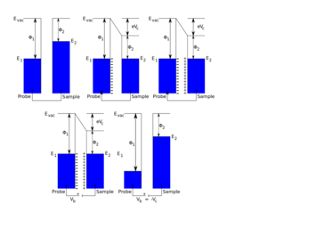
In solid-state physics, the work function is the minimum thermodynamic work needed to remove an electron from a solid to a point in the vacuum immediately outside the solid surface. Here "immediately" means that the final electron position is far from the surface on the atomic scale, but still too close to the solid to be influenced by ambient electric fields in the vacuum. The work function is not a characteristic of a bulk material, but rather a property of the surface of the material.

<span class="mw-page-title-main">Atomic force microscopy</span> Type of microscopy

Atomic force microscopy (AFM) or scanning force microscopy (SFM) is a very-high-resolution type of scanning probe microscopy (SPM), with demonstrated resolution on the order of fractions of a nanometer, more than 1000 times better than the optical diffraction limit.

Scanning probe microscopy (SPM) is a branch of microscopy that forms images of surfaces using a physical probe that scans the specimen. SPM was founded in 1981, with the invention of the scanning tunneling microscope, an instrument for imaging surfaces at the atomic level. The first successful scanning tunneling microscope experiment was done by Gerd Binnig and Heinrich Rohrer. The key to their success was using a feedback loop to regulate gap distance between the sample and the probe.

<span class="mw-page-title-main">Magnetic force microscope</span>

Magnetic force microscopy (MFM) is a variety of atomic force microscopy, in which a sharp magnetized tip scans a magnetic sample; the tip-sample magnetic interactions are detected and used to reconstruct the magnetic structure of the sample surface. Many kinds of magnetic interactions are measured by MFM, including magnetic dipole–dipole interaction. MFM scanning often uses non-contact AFM (NC-AFM) mode.

Electrostatic force microscopy (EFM) is a type of dynamic non-contact atomic force microscopy where the electrostatic force is probed.. This force arises due to the attraction or repulsion of separated charges. It is a long-range force and can be detected 100 nm or more from the sample.

<span class="mw-page-title-main">Chemical force microscopy</span> Method of microscopy which measures chemical bonding between the probe and surface

In materials science, chemical force microscopy (CFM) is a variation of atomic force microscopy (AFM) which has become a versatile tool for characterization of materials surfaces. With AFM, structural morphology is probed using simple tapping or contact modes that utilize van der Waals interactions between tip and sample to maintain a constant probe deflection amplitude or maintain height while measuring tip deflection. CFM, on the other hand, uses chemical interactions between functionalized probe tip and sample. Choice chemistry is typically gold-coated tip and surface with R−SH thiols attached, R being the functional groups of interest. CFM enables the ability to determine the chemical nature of surfaces, irrespective of their specific morphology, and facilitates studies of basic chemical bonding enthalpy and surface energy. Typically, CFM is limited by thermal vibrations within the cantilever holding the probe. This limits force measurement resolution to ~1 pN which is still very suitable considering weak COOH/CH3 interactions are ~20 pN per pair. Hydrophobicity is used as the primary example throughout this consideration of CFM, but certainly any type of bonding can be probed with this method.

<span class="mw-page-title-main">Piezoresponse force microscopy</span> Microscopy technique for piezoelectric materials

Piezoresponse force microscopy (PFM) is a variant of atomic force microscopy (AFM) that allows imaging and manipulation of piezoelectric/ferroelectric materials domains. This is achieved by bringing a sharp conductive probe into contact with a ferroelectric surface and applying an alternating current (AC) bias to the probe tip in order to excite deformation of the sample through the converse piezoelectric effect (CPE). The resulting deflection of the probe cantilever is detected through standard split photodiode detector methods and then demodulated by use of a lock-in amplifier (LiA). In this way topography and ferroelectric domains can be imaged simultaneously with high resolution.

In microscopy, scanning joule expansion microscopy (SJEM) is a form of scanning probe microscopy heavily based on atomic force microscopy (AFM) that maps the temperature distribution along a surface. Resolutions down to 10 nm have been achieved and 1 nm resolution is theoretically possible. Thermal measurements at the nanometer scale are of both academic and industrial interest, particularly in regards to nanomaterials and modern integrated circuits.

<span class="mw-page-title-main">Photoconductive atomic force microscopy</span> Type of atomic force microscopy

Photoconductive atomic force microscopy (PC-AFM) is a variant of atomic force microscopy that measures photoconductivity in addition to surface forces.

Scanning electrochemical microscopy (SECM) is a technique within the broader class of scanning probe microscopy (SPM) that is used to measure the local electrochemical behavior of liquid/solid, liquid/gas and liquid/liquid interfaces. Initial characterization of the technique was credited to University of Texas electrochemist, Allen J. Bard, in 1989. Since then, the theoretical underpinnings have matured to allow widespread use of the technique in chemistry, biology and materials science. Spatially resolved electrochemical signals can be acquired by measuring the current at an ultramicroelectrode (UME) tip as a function of precise tip position over a substrate region of interest. Interpretation of the SECM signal is based on the concept of diffusion-limited current. Two-dimensional raster scan information can be compiled to generate images of surface reactivity and chemical kinetics.

<span class="mw-page-title-main">Atomic force acoustic microscopy</span>

Atomic force acoustic microscopy (AFAM) is a type of scanning probe microscopy (SPM). It is a combination of acoustics and atomic force microscopy. The principal difference between AFAM and other forms of SPM is the addition of a transducer at the bottom of the sample which induces longitudinal out-of-plane vibrations in the specimen. These vibrations are sensed by a cantilever and tip called a probe. The figure shown here is the clear schematic of AFAM principle here B is the magnified version of the tip and sample placed on the transducer and tip having some optical coating generally gold coating to reflect the laser light on to the photodiode.

<span class="mw-page-title-main">Colloidal probe technique</span>

The colloidal probe technique is commonly used to measure interaction forces acting between colloidal particles and/or planar surfaces in air or in solution. This technique relies on the use of an atomic force microscope (AFM). However, instead of a cantilever with a sharp AFM tip, one uses the colloidal probe. The colloidal probe consists of a colloidal particle of few micrometers in diameter that is attached to an AFM cantilever. The colloidal probe technique can be used in the sphere-plane or sphere-sphere geometries. One typically achieves a force resolution between 1 and 100 pN and a distance resolution between 0.5 and 2 nm.

<span class="mw-page-title-main">Non-contact atomic force microscopy</span>

Non-contact atomic force microscopy (nc-AFM), also known as dynamic force microscopy (DFM), is a mode of atomic force microscopy, which itself is a type of scanning probe microscopy. In nc-AFM a sharp probe is moved close to the surface under study, the probe is then raster scanned across the surface, the image is then constructed from the force interactions during the scan. The probe is connected to a resonator, usually a silicon cantilever or a quartz crystal resonator. During measurements the sensor is driven so that it oscillates. The force interactions are measured either by measuring the change in amplitude of the oscillation at a constant frequency just off resonance or by measuring the change in resonant frequency directly using a feedback circuit to always drive the sensor on resonance.

<span class="mw-page-title-main">Infrared Nanospectroscopy (AFM-IR)</span> Infrared microscopy technique

AFM-IR or infrared nanospectroscopy is one of a family of techniques that are derived from a combination of two parent instrumental techniques. AFM-IR combines the chemical analysis power of infrared spectroscopy and the high-spatial resolution of scanning probe microscopy (SPM). The term was first used to denote a method that combined a tuneable free electron laser with an atomic force microscope equipped with a sharp probe that measured the local absorption of infrared light by a sample with nanoscale spatial resolution.

<span class="mw-page-title-main">Nano-FTIR</span> Infrared microscopy technique

Nano-FTIR is a scanning probe technique that utilizes as a combination of two techniques: Fourier transform infrared spectroscopy (FTIR) and scattering-type scanning near-field optical microscopy (s-SNOM). As s-SNOM, nano-FTIR is based on atomic-force microscopy (AFM), where a sharp tip is illuminated by an external light source and the tip-scattered light is detected as a function of tip position. A typical nano-FTIR setup thus consists of an atomic force microscope, a broadband infrared light source used for tip illumination, and a Michelson interferometer acting as Fourier-transform spectrometer. In nano-FTIR, the sample stage is placed in one of the interferometer arms, which allows for recording both amplitude and phase of the detected light. Scanning the tip allows for performing hyperspectral imaging with nanoscale spatial resolution determined by the tip apex size. The use of broadband infrared sources enables the acquisition of continuous spectra, which is a distinctive feature of nano-FTIR compared to s-SNOM. Nano-FTIR is capable of performing infrared (IR) spectroscopy of materials in ultrasmall quantities and with nanoscale spatial resolution. The detection of a single molecular complex and the sensitivity to a single monolayer has been shown. Recording infrared spectra as a function of position can be used for nanoscale mapping of the sample chemical composition, performing a local ultrafast IR spectroscopy and analyzing the nanoscale intermolecular coupling, among others. A spatial resolution of 10 nm to 20 nm is routinely achieved.

A probe tip is an instrument used in scanning probe microscopes (SPMs) to scan the surface of a sample and make nano-scale images of surfaces and structures. The probe tip is mounted on the end of a cantilever and can be as sharp as a single atom. In microscopy, probe tip geometry and the composition of both the tip and the surface being probed directly affect resolution and imaging quality. Tip size and shape are extremely important in monitoring and detecting interactions between surfaces. SPMs can precisely measure electrostatic forces, magnetic forces, chemical bonding, Van der Waals forces, and capillary forces. SPMs can also reveal the morphology and topography of a surface.

Electrochemical AFM (EC-AFM) is a particular type of Scanning probe microscopy (SPM), which combines the classical Atomic force microscopy (AFM) together with electrochemical measurements. EC-AFM allows to perform in-situ AFM measurements in an electrochemical cell, in order to investigate the actual changes in the electrode surface morphology during electrochemical reactions. The solid-liquid interface is thus investigated. This technique was developed for the first time in 1996 by Kouzeki et al., who studied amorphous and polycrystalline thin films of Naphthalocyanine on Indium tin oxide in a solution of 0.1 M Potassium chloride (KCl). Unlike the Electrochemical scanning tunneling microscope, previously developed by Itaya and Tomita in 1988, the tip is non-conductive and it is easily steered in a liquid environment.

Scanning vibrating electrode technique (SVET), also known as vibrating probe within the field of biology, is a scanning probe microscopy (SPM) technique which visualizes electrochemical processes at a sample. It was originally introduced in 1974 by Jaffe and Nuccitelli to investigate the electrical current densities near living cells. Starting in the 1980s Hugh Isaacs began to apply SVET to a number of different corrosion studies. SVET measures local current density distributions in the solution above the sample of interest, to map electrochemical processes in situ as they occur. It utilizes a probe, vibrating perpendicular to the sample of interest, to enhance the measured signal. It is related to scanning ion-selective electrode technique (SIET), which can be used with SVET in corrosion studies, and scanning reference electrode technique (SRET), which is a precursor to SVET.

Scanning quantum dot microscopy (SQDM) is a scanning probe microscopy (SPM) that is used to image nanoscale electric potential distributions on surfaces. The method quantifies surface potential variations via their influence on the potential of a quantum dot (QD) attached to the apex of the scanned probe. SQDM allows, for example, the quantification of surface dipoles originating from individual adatoms, molecules, or nanostructures. This gives insights into surface and interface mechanisms such as reconstruction or relaxation, mechanical distortion, charge transfer and chemical interaction. Measuring electric potential distributions is also relevant for characterizing organic and inorganic semiconductor devices which feature electric dipole layers at the relevant interfaces. The probe to surface distance in SQDM ranges from 2 nm to 10 nm and therefore allows imaging on non-planar surfaces or, e.g., of biomolecules with a distinct 3D structure. Related imaging techniques are Kelvin Probe Force Microscopy (KPFM) and Electrostatic Force Microscopy (EFM).

References

  1. M. Nonnenmacher; M. P. O'Boyle; H. K. Wickramasinghe (1991). "Kelvin probe force microscopy" (PDF). Appl. Phys. Lett. 58 (25): 2921. Bibcode:1991ApPhL..58.2921N. doi:10.1063/1.105227. Archived from the original (free-download pdf) on 2009-09-20.
  2. Fujihira, Masamichi (1999). "Kelvin Probe Force Microscopy of Molecular Surfaces". Annual Review of Materials Science . 29 (1): 353–380. Bibcode:1999AnRMS..29..353F. doi:10.1146/annurev.matsci.29.1.353. ISSN   0084-6600.
  3. Melitz, Wilhelm; Shen, Jian; Kummel, Andrew C.; Lee, Sangyeob (2011). "Kelvin probe force microscopy and its application". Surface Science Reports. 66 (1): 1–27. Bibcode:2011SurSR..66....1M. doi:10.1016/j.surfrep.2010.10.001. ISSN   0167-5729.
  4. Kelvin, Lord (1898). "V. Contact electricity of metals". The London, Edinburgh, and Dublin Philosophical Magazine and Journal of Science. 46 (278): 82–120. doi:10.1080/14786449808621172. ISSN   1941-5982.
  5. Zisman, W. A. (1932). "A New Method of Measuring Contact Potential Differences in Metals". Review of Scientific Instruments. 3 (7): 367–370. Bibcode:1932RScI....3..367Z. doi:10.1063/1.1748947. ISSN   0034-6748.
  6. Rohwerder, Michael; Turcu, Florin (2007). "High-resolution Kelvin probe microscopy in corrosion science: Scanning Kelvin probe force microscopy (SKPFM) versus classical scanning Kelvin probe (SKP)". Electrochimica Acta. 53 (2): 290–299. doi:10.1016/j.electacta.2007.03.016.
  7. Cheran, Larisa-Emilia; Johnstone, Sherri; Sadeghi, Saman; Thompson, Michael (2007-01-19). "Work-function measurement by high-resolution scanning Kelvin nanoprobe". Measurement Science and Technology. 18 (3): 567–578. Bibcode:2007MeScT..18..567C. doi:10.1088/0957-0233/18/3/005. ISSN   0957-0233. S2CID   123457387.
  8. Surplice, N A; D'Arcy, R J (1970). "A critique of the Kelvin method of measuring work functions". Journal of Physics E: Scientific Instruments. 3 (7): 477–482. doi:10.1088/0022-3735/3/7/201. ISSN   0022-3735.
  9. Wagner, Christian; Green, Matthew F. B.; Leinen, Philipp; Deilmann, Thorsten; Krüger, Peter; Rohlfing, Michael; Temirov, Ruslan; Tautz, F. Stefan (2015-07-06). "Scanning Quantum Dot Microscopy". Physical Review Letters. 115 (2): 026101. arXiv: 1503.07738 . Bibcode:2015PhRvL.115b6101W. doi:10.1103/PhysRevLett.115.026101. ISSN   0031-9007. PMID   26207484. S2CID   1720328.
  10. 1 2 Wicinski, Mariusz; Burgstaller, Wolfgang; Hassel, Achim Walter (2016). "Lateral resolution in scanning Kelvin probe microscopy". Corrosion Science. 104: 1–8. doi:10.1016/j.corsci.2015.09.008.
  11. 1 2 McMurray, H. N.; Williams, G. (2002). "Probe diameter and probe–specimen distance dependence in the lateral resolution of a scanning Kelvin probe". Journal of Applied Physics. 91 (3): 1673–1679. Bibcode:2002JAP....91.1673M. doi:10.1063/1.1430546. ISSN   0021-8979.
  12. Huber, Silvia; Wicinski, Mariusz; Hassel, Achim Walter (2018). "Suitability of Various Materials for Probes in Scanning Kelvin Probe Measurements". Physica Status Solidi A. 215 (15): 1700952. Bibcode:2018PSSAR.21500952H. doi: 10.1002/pssa.201700952 .
  13. "High Resolution Scanning Kelvin Probe". Bio-Logic Science Instruments. Retrieved 2019-05-17.
  14. Hansen, Douglas C.; Hansen, Karolyn M.; Ferrell, Thomas L.; Thundat, Thomas (2003). "Discerning Biomolecular Interactions Using Kelvin Probe Technology". Langmuir. 19 (18): 7514–7520. doi:10.1021/la034333w. ISSN   0743-7463.
  15. Dirscherl, Konrad; Baikie, Iain; Forsyth, Gregor; Heide, Arvid van der (2003). "Utilisation of a micro-tip scanning Kelvin probe for non-invasive surface potential mapping of mc-Si solar cells". Solar Energy Materials and Solar Cells. 79 (4): 485–494. doi:10.1016/S0927-0248(03)00064-3.
  16. Stratmann, M. (1987). "The investigation of the corrosion properties of metals, covered with adsorbed electrolyte layers—A new experimental technique". Corrosion Science. 27 (8): 869–872. doi:10.1016/0010-938X(87)90043-6.
  17. Nazarov, A. P.; Thierry, D. (2001). "Study of the Carbon Steel/Alkyd Coating Interface with a Scanning Vibrating Capacitor Technique". Protection of Metals. 37 (2): 108–119. doi:10.1023/a:1010361702449. ISSN   0033-1732. S2CID   92117439.
  18. "Height tracking with the SKP370 or SKP470 module" (PDF). Bio-Logic Science Instruments. Retrieved 2019-05-17.
  19. Wapner, K.; Schoenberger, B.; Stratmann, M.; Grundmeier, G. (2005). "Height-Regulating Scanning Kelvin Probe for Simultaneous Measurement of Surface Topology and Electrode Potentials at Buried Polymer/Metal Interfaces". Journal of the Electrochemical Society. 152 (3): E114. Bibcode:2005JElS..152E.114W. doi:10.1149/1.1856914.
  20. Fernández Garrillo, P. A.; Grévin, B.; Chevalier, N.; Borowik, Ł. (2018). "Calibrated work function mapping by Kelvin probe force microscopy" (PDF). Review of Scientific Instruments. 89 (4): 043702. Bibcode:2018RScI...89d3702F. doi:10.1063/1.5007619. PMID   29716375.
  21. "SKP imaging example of a corroded Zn-plated Fe sample" (PDF). Bio-Logic Science Instruments. Retrieved 2019-05-17.
  22. Fan, Weijie; Zhang, Yong; Li, Weihua; Wang, Wei; Zhao, Xiaodong; Song, Liying (2019). "Multi-level self-healing ability of shape memory polyurethane coating with microcapsules by induction heating". Chemical Engineering Journal. 368: 1033–1044. doi:10.1016/j.cej.2019.03.027. S2CID   104432686.
  23. Borth, David J.; Iezzi, Erick B.; Dudis, Douglas S.; Hansen, Douglas C. (2019). "Nondestructive Evaluation of Urethane-Ester Coating Systems Using the Scanning Kelvin Probe Technique". Corrosion. 75 (5): 457–464. doi:10.5006/3020. ISSN   0010-9312. S2CID   105314795.
  24. Zhang, Dawei; Zhou, Feichi; Xiao, Kui; Cui, Tianyu; Qian, Hongchong; Li, Xiaogang (2015). "Microbially Influenced Corrosion of 304 Stainless Steel and Titanium by P. variotii and A. niger in Humid Atmosphere". Journal of Materials Engineering and Performance. 24 (7): 2688–2698. Bibcode:2015JMEP...24.2688Z. doi:10.1007/s11665-015-1558-2. ISSN   1059-9495. S2CID   137116966.
  25. Szklarska, M.; Dercz, G.; Kubisztal, J.; Balin, K.; Łosiewicz, B. (2016). "Semi-Conducting Properties of Titanium Dioxide Layer on Surface of Ti-15Mo Implant Alloy in Biological Milieu". Acta Physica Polonica A. 130 (4): 1085–1087. Bibcode:2016AcPPA.130.1085S. doi: 10.12693/APhysPolA.130.1085 . ISSN   0587-4246.
  26. Kong, Decheng; Dong, Chaofang; Ni, Xiaoqing; Man, Cheng; Xiao, Kui; Li, Xiaogang (2018). "Insight into the mechanism of alloying elements (Sn, Be) effect on copper corrosion during long-term degradation in harsh marine environment". Applied Surface Science. 455: 543–553. Bibcode:2018ApSS..455..543K. doi: 10.1016/j.apsusc.2018.06.029 . S2CID   102769318.
  27. Jin, Z.H.; Ge, H.H.; Lin, W.W.; Zong, Y.W.; Liu, S.J.; Shi, J.M. (2014). "Corrosion behaviour of 316L stainless steel and anti-corrosion materials in a high acidified chloride solution". Applied Surface Science. 322: 47–56. Bibcode:2014ApSS..322...47J. doi:10.1016/j.apsusc.2014.09.205.
  28. Dirscherl, Konrad; Baikie, Iain; Forsyth, Gregor; Heide, Arvid van der (2003). "Utilisation of a micro-tip scanning Kelvin probe for non-invasive surface potential mapping of mc-Si solar cells". Solar Energy Materials and Solar Cells. 79 (4): 485–494. doi:10.1016/s0927-0248(03)00064-3. ISSN   0927-0248.
  29. Liu, Xiangyang; Zheng, Haiwu; Zhang, Jiwei; Xiao, Yin; Wang, Zhiyong (2013). "Photoelectric properties and charge dynamics for a set of solid state solar cells with Cu4Bi4S9 as the absorber layer". Journal of Materials Chemistry A. 1 (36): 10703. doi:10.1039/c3ta11830d. ISSN   2050-7488.
  30. Williams, Geraint; McMurray, H. N. (2008). "Human Fingerprint - Metal Interactions Studied Using a Scanning Kelvin Probe". ECS Transactions. Washington, DC: ECS. 11 (22): 81–89. Bibcode:2008ECSTr..11v..81W. doi:10.1149/1.2925265. S2CID   98393112.
  31. Bryant, David E.; Greenfield, David; Walshaw, Richard D.; Evans, Suzanne M.; Nimmo, Alexander E.; Smith, Caroline L.; Wang, Liming; Pasek, Matthew A.; Kee, Terence P. (2009). "Electrochemical studies of iron meteorites: phosphorus redox chemistry on the early Earth". International Journal of Astrobiology. 8 (1): 27–36. Bibcode:2009IJAsB...8...27B. doi:10.1017/S1473550408004345. ISSN   1473-5504. S2CID   97821022.
  32. Bryant, David E.; Greenfield, David; Walshaw, Richard D.; Johnson, Benjamin R.G.; Herschy, Barry; Smith, Caroline; Pasek, Matthew A.; Telford, Richard; Scowen, Ian (2013). "Hydrothermal modification of the Sikhote-Alin iron meteorite under low pH geothermal environments. A plausibly prebiotic route to activated phosphorus on the early Earth". Geochimica et Cosmochimica Acta. 109: 90–112. Bibcode:2013GeCoA.109...90B. doi:10.1016/j.gca.2012.12.043.
  33. Nuccitelli, Richard; Nuccitelli, Pamela; Ramlatchan, Samdeo; Sanger, Richard; Smith, Peter J.S. (2008). "Imaging the electric field associated with mouse and human skin wounds". Wound Repair and Regeneration. 16 (3): 432–441. doi:10.1111/j.1524-475X.2008.00389.x. ISSN   1067-1927. PMC   3086402 . PMID   18471262.
  34. Gow, Brian J.; Cheng, Justine L.; Baikie, Iain D.; Martinsen, Ørjan G.; Zhao, Min; Smith, Stephanie; Ahn, Andrew C. (2012). "Electrical Potential of Acupuncture Points: Use of a Noncontact Scanning Kelvin Probe". Evidence-Based Complementary and Alternative Medicine. 2012: 632838. doi: 10.1155/2012/632838 . ISSN   1741-427X. PMC   3541002 . PMID   23320033.
  35. Tzeng, S.-D.; Gwo, S. (2006-07-15). "Charge trapping properties at silicon nitride/silicon oxide interface studied by variable-temperature electrostatic force microscopy". Journal of Applied Physics. 100 (2): 023711–023711–9. Bibcode:2006JAP...100b3711T. doi: 10.1063/1.2218025 . ISSN   0021-8979.
  36. Khosla, Robin; Kumar, Pawan; Sharma, Satinder K. (December 2015). "Charge Trapping and Decay Mechanism in Post Deposition Annealed Er2O3 MOS Capacitors by Nanoscopic and Macroscopic Characterization". IEEE Transactions on Device and Materials Reliability. 15 (4): 610–616. doi:10.1109/TDMR.2015.2498310. ISSN   1530-4388. S2CID   33548746.
  37. Khosla, Robin; Rolseth, Erlend Granbo; Kumar, Pawan; Vadakupudhupalayam, Senthil Srinivasan; Sharma, Satinder K.; Schulze, Jorg (March 2017). "Charge Trapping Analysis of Metal/Al 2 O 3 /SiO 2 /Si, Gate Stack for Emerging Embedded Memories". IEEE Transactions on Device and Materials Reliability. 17 (1): 80–89. doi:10.1109/TDMR.2017.2659760. ISSN   1530-4388. S2CID   24247825.