Low-energy electron microscopy

Last updated
A low-energy electron microscope used for surface science studies at University of Illinois' Frederick Seitz Materials Research Laboratory in Urbana, IL, USA. UIUC LEEM.jpg
A low-energy electron microscope used for surface science studies at University of Illinois' Frederick Seitz Materials Research Laboratory in Urbana, IL, USA.

Low-energy electron microscopy, or LEEM, is an analytical surface science technique used to image atomically clean surfaces, atom-surface interactions, and thin (crystalline) films. [1] In LEEM, high-energy electrons (15-20 keV) are emitted from an electron gun, focused using a set of condenser optics, and sent through a magnetic beam deflector (usually 60˚ or 90˚). The “fast” electrons travel through an objective lens and begin decelerating to low energies (1-100 eV) near the sample surface because the sample is held at a potential near that of the gun. The low-energy electrons are now termed “surface-sensitive” and the near-surface sampling depth can be varied by tuning the energy of the incident electrons (difference between the sample and gun potentials minus the work functions of the sample and system). The low-energy elastically backscattered electrons travel back through the objective lens, reaccelerate to the gun voltage (because the objective lens is grounded), and pass through the beam separator again. However, now the electrons travel away from the condenser optics and into the projector lenses. Imaging of the back focal plane of the objective lens into the object plane of the projector lens (using an intermediate lens) produces a diffraction pattern (low-energy electron diffraction, LEED) at the imaging plane and recorded in a number of different ways. The intensity distribution of the diffraction pattern will depend on the periodicity at the sample surface and is a direct result of the wave nature of the electrons. One can produce individual images of the diffraction pattern spot intensities by turning off the intermediate lens and inserting a contrast aperture in the back focal plane of the objective lens (or, in state-of-the-art instruments, in the center of the separator, as chosen by the excitation of the objective lens), thus allowing for real-time observations of dynamic processes at surfaces. Such phenomena include (but are not limited to): tomography, phase transitions, adsorption, reaction, segregation, thin film growth, etching, strain relief, sublimation, and magnetic microstructure. These investigations are only possible because of the accessibility of the sample; allowing for a wide variety of in situ studies over a wide temperature range. LEEM was invented by Ernst Bauer in 1962; however, not fully developed (by Ernst Bauer and Wolfgang Telieps) until 1985.

Contents

Introduction

LEEM differs from conventional electron microscopes in four main ways:

  1. The sample must be illuminated on the same side of the imaging optics, i.e. through the objective lens, because samples are not transparent to low-energy electrons;
  2. In order to separate the incident and elastically scattered low energy electrons, scientists use magnetic “electron prism” beam separators which focus electrons both in and out of the plane of the beampath (to avoid distortions in the image and diffraction patterns);
  3. In electrostatic immersion objective lens brings the sample close to that of the gun, slowing down the high energy electrons to a desired energy only just before interacting with the sample surface;
  4. The instrument must be able to work under ultra-high vacuum (UHV), or 10−10 torr (760 torr = 1 atm, atmospheric pressure), although "near-ambient pressure" (NAP-LEEM) instruments have been developed by adding a higher pressure compartment and differential pumping stages, allowing for sample room pressures up to 10−1 mbar. [2]

Surface diffraction

Ewald's sphere construction for the case of normal incidence of the primary electron beam. Here, this is done in a typical LEED set-up, however, in LEEM, there are complicated electron optics that allow for imaging of the resultant diffraction patterns and hence, the surface of the sample. EwaldsphereLEED.png
Ewald's sphere construction for the case of normal incidence of the primary electron beam. Here, this is done in a typical LEED set-up, however, in LEEM, there are complicated electron optics that allow for imaging of the resultant diffraction patterns and hence, the surface of the sample.

Kinematic or elastic backscattering occurs when low energy (1-100 eV) electrons impinge on a clean, well-ordered crystalline specimen. It is assumed that each electron undergoes only one scattering event, and incident electron beam is described as a plane wave with the wavelength:

Inverse space is used to describe the periodicity of the lattice and the interaction of the plane wave with the sample surface. In inverse (or "k-space") space, the wave vector of the incident and scattered waves are and , respectively,

and constructive interference occurs at the Laue condition:

where (h,k,l) is a set of integers and

is a vector of the reciprocal lattice.

Experimental setup

A typical LEEM/LEED lens and ray diagram. LEED Lens and Ray Diagram.png
A typical LEEM/LEED lens and ray diagram.

A typical LEEM setup consists of electron gun, used to generate electrons by way of thermionic or field emission from a source tip. In thermionic emission, electrons escape a source tip (usually made of LaB6) by resistive heating and application of an electric field to effectively lower the energy needed for electrons to escape the surface. Once sufficient thermal vibrational energy is attained electrons may overcome this electrostatic energy barrier, allowing them to travel into vacuum and accelerate down the lens column to the gun potential (because the lenses are at ground). In field emission, rather than heating the tip to vibrationally excite electrons from the surface, the source tip (usually tungsten) is sharpened to a small point such that when large electric fields are applied, they concentrate at the tip, lowering the barrier to escape the surface as well as making tunneling of electrons from the tip to vacuum level more feasible.

Condenser/illumination optics are used to focus electrons leaving the electron gun and manipulate and/or translate the illumination electron beam. Electromagnetic quadrupole electron lenses are used, the number of which depends on how much resolution and focusing flexibility the designer wishes. However, the ultimate resolution of LEEM is usually determined by that of the objective lens.

Illumination beam aperture allows researchers to control the area of the specimen which is illuminated (LEEM's version of electron microscopy's “selected area diffraction”, termed microdiffraction) and is located in the beam separator on the illumination side.

Magnetic beam separator is needed to resolve the illuminating and imaging beam (while in turn spatially separating the optics for each). There has been much development on the technology of electron beam separators; the early separators introduced distortion in either the image or diffraction plane. However, IBM recently developed a hybrid prism array/nested quadratic field design, focusing the electron beams both in and out of the plane of the beampath, allowing for deflection and transfer of the image and diffraction planes without distortion or energy dispersion.

Electrostatic immersion objective lens is used to form a real image of the sample by way of a 2/3-magnification virtual image behind the sample. The uniformity of the electrostatic field between the objective lens and specimen, limited by spherical and chromatic aberrations larger than those of any other lenses, ultimately determines the overall performance of the instrument.

Contrast aperture is located in the center on the projector lens side of the beam separator. In most electron microscopies, the contrast aperture is introduced into the back focal plan of the objective lens (where the actual diffraction plane lies). However, this is not true in the LEEM, because dark-field imaging (imaging of nonspecular beams) would not be possible because the aperture has to move laterally and would intercept the incident beam for large shifts. Therefore, researchers adjust the excitation of the objective lens so as to produce an image of the diffraction pattern in the middle of the beam separator and choose the desired spot intensity to image using a contrast aperture inserted there. This aperture allows scientists to image diffraction intensities that may be of particular interest (dark field).

Illumination optics are employed to magnify the image or diffraction pattern and project it onto the imaging plate or screen. Imaging plate or screen used to image the electron intensity so that we can see it. This can be done many different ways including, phosphorescent screens, imaging plates, CCDs, among others.

Specialized imaging techniques

LEEM bright-field (step/phase contrast) image of Cr(100). Atomic steps, step bunches, islands and terraces are easily discernible from vertical diffraction contrast originating from the wave nature of electrons. Field of view is 5.6 mm. Cr(001).png
LEEM bright-field (step/phase contrast) image of Cr(100). Atomic steps, step bunches, islands and terraces are easily discernible from vertical diffraction contrast originating from the wave nature of electrons. Field of view is 5.6 μm.
The LEEM image corresponding to a sub-monolayer palladium film (dark contrast) grown on the (110) surface of a tungsten crystal (bright contrast). The barely visible islands are tungsten carbides due to carbon contamination. Diameter of the imaged area is 10 micrometres. LEEM palladium on tungsten.jpg
The LEEM image corresponding to a sub-monolayer palladium film (dark contrast) grown on the (110) surface of a tungsten crystal (bright contrast). The barely visible islands are tungsten carbides due to carbon contamination. Diameter of the imaged area is 10 micrometres.

Low energy electron diffraction (LEED)

After a parallel beam of low-energy electrons interacts with a specimen, the electrons form a diffraction or LEED pattern which depends on periodicity present at the surface and is a direct result of the wave nature of an electron. It is important to point out that in regular LEED the entire sample surface is being illuminated by a parallel beam of electrons, and thus the diffraction pattern will contain information about the entire surface.

LEED performed in a LEEM instrument (sometimes referred to as Very Low-Energy Electron Diffraction (VLEED), due to the even lower electron energies), limits the area illuminated to the beam spot, typically in the order of square micrometers. The diffraction pattern is formed in the back focal plane of the objective lens, imaged into the object plane of the projective lens (using an intermediate lens), and the final pattern appears on the phosphorescent screen, photographic plate or CCD.

As the reflected electrons are bent away from the electron source by the prism, the specular reflected electrons can be measured, even starting from zero landing energy, as no shadow of the source is visible on the screen (which prevents this in regular LEED instruments). It is worth noting that the spacing of diffracted beams does not increase with kinetic energy as for conventional LEED systems. This is due to the imaged electrons being accelerated to the high energy of the imaging column and are therefore imaged with a constant size of K-space regardless of the incident electron energy.

Microdiffraction

Microdiffraction is conceptually exactly like LEED. However, unlike in a LEED experiment where the sampled surface area is some square millimeters, one inserts the illumination and the beam aperture into the beam path while imaging a surface and thus reduces the size of the sampled surface area. The chosen area ranges from a fraction of a square micrometer to square micrometers. If the surface is not homogeneous, a diffraction pattern obtained from LEED experiment appears convoluted and is therefore hard to analyze. In a microdiffraction experiment researchers may focus on a particular island, terrace, domain and so on, and retrieve a diffraction pattern composed solely of a single surface feature, making the technique extremely useful.

Graphene on SiC is composed of domains of different stacking order. (left) Bright-field LEEM micrograph of a samples of bilayer, trilayer, and four-layer intercalated graphene. (right) Dark-field images of the same area. Domains of alternating contrast are clearly visible, indicating areas of different stacking order. Adapted from GrapheneonSiC-brightfield-darkfield-LEEM.png
Graphene on SiC is composed of domains of different stacking order. (left) Bright-field LEEM micrograph of a samples of bilayer, trilayer, and four-layer intercalated graphene. (right) Dark-field images of the same area. Domains of alternating contrast are clearly visible, indicating areas of different stacking order. Adapted from

Bright field imaging

Bright Field imaging uses the specular, reflected, (0,0) beam to form an image. Also known as phase or interference contrast imaging, bright field imaging makes particular use of the wave nature of the electron to generate vertical diffraction contrast, making steps on the surface visible.

Dark field imaging

In dark field imaging (also termed diffraction contrast imaging) researchers choose a desired diffraction spot and use a contrast aperture to pass only those electrons that contribute to that particular spot. In the image planes after the contrast aperture it is then possible to observe where the electrons originate from in real space. This technique allows scientists to study on which areas of a specimen a structure with a certain lattice vector (periodicity) exists.

Spectroscopy

Both (micro-)diffraction as well as bright field and dark field imaging can be performed as a function of the electron landing energy, measuring a diffraction pattern or an image for a range of energies. This way of measuring (often called LEEM-IV) yields spectra for each diffraction spot or sample position. In its simplest form, this spectrum gives a `fingerprint' of the surface, enabling the identification of different surface structures.

A particular application of bright field spectroscopy is the counting of the exact number of layers in layered materials such as (few layer) graphene, hexagonal boron nitride and some transition metal dichalcogenides. [4] [5] [6]

Photoexcitation electron microscopy (PEEM) of Ag rods on Si. Here, an Hg lamp produces photons of energy just above the work function threshold of Ag, and the resultant secondary electron emission is imaged. Ag rods on Si.png
Photoexcitation electron microscopy (PEEM) of Ag rods on Si. Here, an Hg lamp produces photons of energy just above the work function threshold of Ag, and the resultant secondary electron emission is imaged.

Photoemission electron microscopy (PEEM)

In photoemission electron microscopy (PEEM), upon exposure to electromagnetic radiation (photons), secondary electrons are excited from the surface and imaged. PEEM was first developed in the early 1930s, using ultraviolet (UV) light to induce photoemission of (secondary) electrons. However, since then, this technique has made many advances, the most important of which was the pairing of PEEM with a synchrotron light source, providing tunable, linear polarized, left and right circularized radiation in the soft x-ray range. Such application allows scientist to retrieve topographical, elemental, chemical, and magnetic contrast of surfaces.

LEEM instruments are often equipped with light sources to perform PEEM imaging. This helps in system alignment and enables collection LEEM, PEEM and ARPES data of a single sample in a single instrument.

Mirror electron microscopy (MEM)

In mirror electron microscopy, electrons are slowed in the retarding field of the condenser lens to the limit of the instrument and thus, only allowed to interact with the “near-surface” region of the sample. It is very complicated to understand the exact contrast variations come from, but the important things to point out here are that height variations at the surface of the region change the properties of the retarding field, therefore influencing the reflected (specular) beam. No LEED pattern is formed, because no scattering events have taken place, and therefore, reflected intensity is high.

Low-energy electron holography

Low-energy electron holography of DNA molecules stretched over lacey carbon. Adapted from Latychevskaia et al. Low-energy electron holography.jpg
Low-energy electron holography of DNA molecules stretched over lacey carbon. Adapted from Latychevskaia et al.

Low-energy electron holography [8] is realized with electron with kinetic energies in the range 30 - 250 eV. The source of the coherent electron beam is a sharp metal tip and the electrons are extracted by field emission. The wave transmitted through the sample propagates to the detector where the interference pattern is acquired, formed by superposition of the scattered with the non-scattered (reference) wave, constituting an in-line hologram. The structure of the object (macromolecule) is then reconstructed from the hologram by numerical methods. Low-energy electron holography has successfully been applied for imaging of individual biological molecules, including: purple protein membrane, DNA molecules, phthalocyaninato polysiloxane molecules, the tobacco mosaic virus8, a bacteriophage, ferritin and individual proteins (bovine serum albumin, cytochrome C and hemoglobin). The resolution achieved by low-energy electron holography is about 0.7 - 1 nm. [7]

Reflectivity contrast imaging

The elastic backscattering of low energy electrons from surfaces is strong. The reflectivity coefficients of surfaces depend strongly on the energy of incident electrons and the nuclear charge, in a non-monotonic fashion. Therefore, contrast can be maximized by varying the energy of the electrons incident at the surface.

Spin-polarized LEEM (SPLEEM)

SPLEEM uses spin-polarized illumination electrons to image the magnetic structure of a surface by way of spin-spin coupling of the incident electrons with that of the surface.

Other

Other advanced techniques include: [4]

Related Research Articles

<span class="mw-page-title-main">Electron microscope</span> Type of microscope with electrons as a source of illumination

An electron microscope is a microscope that uses a beam of electrons as a source of illumination. They use electron optics that are analogous to the glass lenses of an optical light microscope to control the electron beam, for instance focusing them to produce magnified images or electron diffraction patterns. As the wavelength of an electron can be up to 100,000 times smaller than that of visible light, electron microscopes have a much higher resolution of about 0.1 nm, which compares to about 200 nm for light microscopes. Electron microscope may refer to:

<span class="mw-page-title-main">Microscopy</span> Viewing of objects which are too small to be seen with the naked eye

Microscopy is the technical field of using microscopes to view objects and areas of objects that cannot be seen with the naked eye. There are three well-known branches of microscopy: optical, electron, and scanning probe microscopy, along with the emerging field of X-ray microscopy.

<span class="mw-page-title-main">Microscope</span> Scientific instrument

A microscope is a laboratory instrument used to examine objects that are too small to be seen by the naked eye. Microscopy is the science of investigating small objects and structures using a microscope. Microscopic means being invisible to the eye unless aided by a microscope.

<span class="mw-page-title-main">Optical microscope</span> Microscope that uses visible light

The optical microscope, also referred to as a light microscope, is a type of microscope that commonly uses visible light and a system of lenses to generate magnified images of small objects. Optical microscopes are the oldest design of microscope and were possibly invented in their present compound form in the 17th century. Basic optical microscopes can be very simple, although many complex designs aim to improve resolution and sample contrast.

<span class="mw-page-title-main">Transmission electron microscopy</span> Imaging and diffraction using electrons that pass through samples

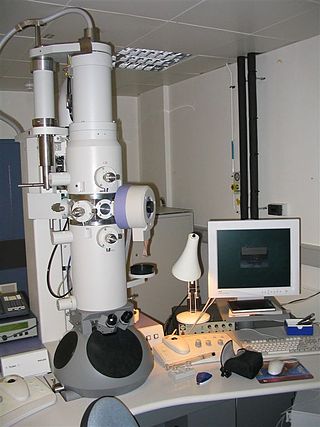
Transmission electron microscopy (TEM) is a microscopy technique in which a beam of electrons is transmitted through a specimen to form an image. The specimen is most often an ultrathin section less than 100 nm thick or a suspension on a grid. An image is formed from the interaction of the electrons with the sample as the beam is transmitted through the specimen. The image is then magnified and focused onto an imaging device, such as a fluorescent screen, a layer of photographic film, or a detector such as a scintillator attached to a charge-coupled device or a direct electron detector.

<span class="mw-page-title-main">Electron diffraction</span> Bending of electron beams due to electrostatic interactions with matter

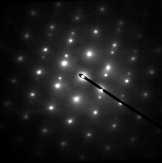
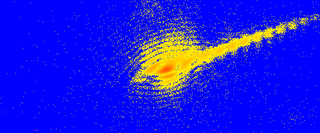
Electron diffraction is a generic term for phenomena associated with changes in the direction of electron beams due to elastic interactions with atoms. It occurs due to elastic scattering, when there is no change in the energy of the electrons. The negatively charged electrons are scattered due to Coulomb forces when they interact with both the positively charged atomic core and the negatively charged electrons around the atoms. The resulting map of the directions of the electrons far from the sample is called a diffraction pattern, see for instance Figure 1. Beyond patterns showing the directions of electrons, electron diffraction also plays a major role in the contrast of images in electron microscopes.

<span class="mw-page-title-main">Diffraction-limited system</span> Optical system with resolution performance at the instruments theoretical limit

In optics, any optical instrument or system – a microscope, telescope, or camera – has a principal limit to its resolution due to the physics of diffraction. An optical instrument is said to be diffraction-limited if it has reached this limit of resolution performance. Other factors may affect an optical system's performance, such as lens imperfections or aberrations, but these are caused by errors in the manufacture or calculation of a lens, whereas the diffraction limit is the maximum resolution possible for a theoretically perfect, or ideal, optical system.

Photoemission electron microscopy is a type of electron microscopy that utilizes local variations in electron emission to generate image contrast. The excitation is usually produced by ultraviolet light, synchrotron radiation or X-ray sources. PEEM measures the coefficient indirectly by collecting the emitted secondary electrons generated in the electron cascade that follows the creation of the primary core hole in the absorption process. PEEM is a surface sensitive technique because the emitted electrons originate from a shallow layer. In physics, this technique is referred to as PEEM, which goes together naturally with low-energy electron diffraction (LEED), and low-energy electron microscopy (LEEM). In biology, it is called photoelectron microscopy (PEM), which fits with photoelectron spectroscopy (PES), transmission electron microscopy (TEM), and scanning electron microscopy (SEM).

<span class="mw-page-title-main">Confocal microscopy</span> Optical imaging technique

Confocal microscopy, most frequently confocal laser scanning microscopy (CLSM) or laser scanning confocal microscopy (LSCM), is an optical imaging technique for increasing optical resolution and contrast of a micrograph by means of using a spatial pinhole to block out-of-focus light in image formation. Capturing multiple two-dimensional images at different depths in a sample enables the reconstruction of three-dimensional structures within an object. This technique is used extensively in the scientific and industrial communities and typical applications are in life sciences, semiconductor inspection and materials science.

<span class="mw-page-title-main">Scanning transmission electron microscopy</span> Scanning microscopy using thin samples and transmitted electrons

A scanning transmission electron microscope (STEM) is a type of transmission electron microscope (TEM). Pronunciation is [stɛm] or [ɛsti:i:ɛm]. As with a conventional transmission electron microscope (CTEM), images are formed by electrons passing through a sufficiently thin specimen. However, unlike CTEM, in STEM the electron beam is focused to a fine spot which is then scanned over the sample in a raster illumination system constructed so that the sample is illuminated at each point with the beam parallel to the optical axis. The rastering of the beam across the sample makes STEM suitable for analytical techniques such as Z-contrast annular dark-field imaging, and spectroscopic mapping by energy dispersive X-ray (EDX) spectroscopy, or electron energy loss spectroscopy (EELS). These signals can be obtained simultaneously, allowing direct correlation of images and spectroscopic data.

<span class="mw-page-title-main">Selected area diffraction</span>

Selected area (electron) diffraction is a crystallographic experimental technique typically performed using a transmission electron microscope (TEM). It is a specific case of electron diffraction used primarily in material science and solid state physics as one of the most common experimental techniques. Especially with appropriate analytical software, SAD patterns (SADP) can be used to determine crystal orientation, measure lattice constants or examine its defects.

X-ray optics is the branch of optics that manipulates X-rays instead of visible light. It deals with focusing and other ways of manipulating the X-ray beams for research techniques such as X-ray crystallography, X-ray fluorescence, small-angle X-ray scattering, X-ray microscopy, X-ray phase-contrast imaging, and X-ray astronomy.

<span class="mw-page-title-main">High-resolution transmission electron microscopy</span>

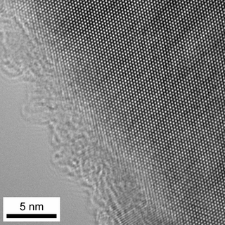
High-resolution transmission electron microscopy is an imaging mode of specialized transmission electron microscopes that allows for direct imaging of the atomic structure of samples. It is a powerful tool to study properties of materials on the atomic scale, such as semiconductors, metals, nanoparticles and sp2-bonded carbon. While this term is often also used to refer to high resolution scanning transmission electron microscopy, mostly in high angle annular dark field mode, this article describes mainly the imaging of an object by recording the two-dimensional spatial wave amplitude distribution in the image plane, similar to a "classic" light microscope. For disambiguation, the technique is also often referred to as phase contrast transmission electron microscopy, although this term is less appropriate. At present, the highest point resolution realised in high resolution transmission electron microscopy is around 0.5 ångströms (0.050 nm). At these small scales, individual atoms of a crystal and defects can be resolved. For 3-dimensional crystals, it is necessary to combine several views, taken from different angles, into a 3D map. This technique is called electron tomography.

<span class="mw-page-title-main">Low-energy electron diffraction</span> Technique for determining surface structures

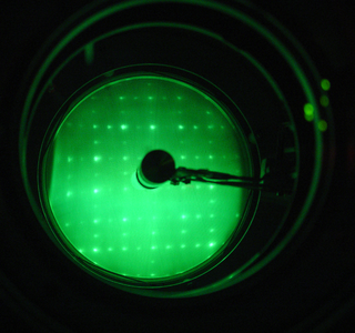
Low-energy electron diffraction (LEED) is a technique for the determination of the surface structure of single-crystalline materials by bombardment with a collimated beam of low-energy electrons (30–200 eV) and observation of diffracted electrons as spots on a fluorescent screen.

<span class="mw-page-title-main">Dark-field microscopy</span> Laboratory technique

Dark-field microscopy describes microscopy methods, in both light and electron microscopy, which exclude the unscattered beam from the image. Consequently, the field around the specimen is generally dark.

<span class="mw-page-title-main">Coherent diffraction imaging</span>

Coherent diffractive imaging (CDI) is a "lensless" technique for 2D or 3D reconstruction of the image of nanoscale structures such as nanotubes, nanocrystals, porous nanocrystalline layers, defects, potentially proteins, and more. In CDI, a highly coherent beam of X-rays, electrons or other wavelike particle or photon is incident on an object.

<span class="mw-page-title-main">Ernst G. Bauer</span> German-American physicist

Ernst G. Bauer is a German-American physicist known for his studies in the field of surface science, thin film growth and nucleation mechanisms and the invention in 1962 of the Low Energy Electron Microscopy (LEEM). In the early 1990s, he extended the LEEM technique in two directions by developing Spin-Polarized Low Energy Electron Microscopy (SPLEEM) and Spectroscopic Photo Emission and Low Energy Electron Microscopy (SPELEEM). He is currently Distinguished Research Professor Emeritus at the Arizona State University.

<span class="mw-page-title-main">Ptychography</span>

Ptychography is a computational method of microscopic imaging. It generates images by processing many coherent interference patterns that have been scattered from an object of interest. Its defining characteristic is translational invariance, which means that the interference patterns are generated by one constant function moving laterally by a known amount with respect to another constant function. The interference patterns occur some distance away from these two components, so that the scattered waves spread out and "fold" into one another as shown in the figure.

<span class="mw-page-title-main">Optical sectioning</span> Imaging of focal planes within a thick sample

Optical sectioning is the process by which a suitably designed microscope can produce clear images of focal planes deep within a thick sample. This is used to reduce the need for thin sectioning using instruments such as the microtome. Many different techniques for optical sectioning are used and several microscopy techniques are specifically designed to improve the quality of optical sectioning.

References

  1. Bauer, E (1994). "Low energy electron microscopy". Reports on Progress in Physics. 57 (9): 895–938. Bibcode:1994RPPh...57..895B. doi:10.1088/0034-4885/57/9/002. ISSN   0034-4885. S2CID   250913078.
  2. Franz, Torsten; von Boehn, Bernhard; Marchetto, Helder; Borkenhagen, Benjamin; Lilienkamp, Gerhard; Daum, Winfried; Imbihl, Ronald (2019). "Catalytic CO oxidation on Pt under near ambient pressure: A NAP-LEEM study". Ultramicroscopy. 200. Elsevier BV: 73–78. doi:10.1016/j.ultramic.2019.02.024. ISSN   0304-3991. PMID   30836286. S2CID   73480940.
  3. de Jong, T. A.; Krasovskii, E. E.; Ott, C.; Tromp, R. M.; van der Molen, S. J.; Jobst, J. (2018-10-31). "Intrinsic stacking domains in graphene on silicon carbide: A pathway for intercalation". Physical Review Materials. 2 (10). American Physical Society (APS): 104005. arXiv: 1807.04185 . doi: 10.1103/physrevmaterials.2.104005 . ISSN   2475-9953.
  4. 1 2 Tromp, Rudolf (2019). "Spectroscopy with the Low Energy Electron Microscope". In Hawkes, Peter W.; Spence, John C. H. (eds.). Springer Handbook of Microscopy. Springer Handbooks. Springer International Publishing. pp. 576–581. doi:10.1007/978-3-030-00069-1_11. ISBN   978-3-030-00069-1. S2CID   210235774.
  5. de la Barrera, Sergio C.; Lin, Yu-Chuan; Eichfeld, Sarah M.; Robinson, Joshua A.; Gao, Qin; Widom, Michael; Feenstra, Randall M. (July 2016). "Thickness characterization of atomically thin WSe2 on epitaxial graphene by low-energy electron reflectivity oscillations". Journal of Vacuum Science & Technology B, Nanotechnology and Microelectronics: Materials, Processing, Measurement, and Phenomena. 34 (4). American Vacuum Society: 04J106. arXiv: 1606.04167 . doi: 10.1116/1.4954642 .
  6. de Jong, Tobias A.; Jobst, Johannes; Yoo, Hyobin; Krasovskii, Eugene E.; Kim, Philip; van der Molen, Sense Jan (2018). "Measuring the Local Twist Angle and Layer Arrangement in Van der Waals Heterostructures". Physica Status Solidi B. 255 (12). Wiley: 1800191. doi: 10.1002/pssb.201800191 . hdl: 1887/62920 .
  7. 1 2 Latychevskaia, T.; Escher, C.; Andregg, W.; Andregg, M.; Fink, H.-W. (20 June 2019). "Direct visualization of charge transport in suspended (or free-standing) DNA strands by low-energy electron microscopy". Scientific Reports. 9 (1). Nature: 8889. doi: 10.1038/s41598-019-45351-4 . PMC   6586886 . PMID   31222124. CC-BY icon.svg Text was copied from this source, which is available under a Creative Commons Attribution 4.0 International License.
  8. Fink, H.-W; Stocker, W.; Schmid, H. (30 May 1990). "Holography with low-energy electrons". Phys. Rev. Lett. 65 (10). American Physical Society: 1204–1206. doi:10.1103/PhysRevLett.65.1204. PMID   10042201.