Microscopy is the technical field of using microscopes to view objects and areas of objects that cannot be seen with the naked eye. There are three well-known branches of microscopy: optical, electron, and scanning probe microscopy, along with the emerging field of X-ray microscopy.

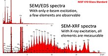
A scanning electron microscope (SEM) is a type of electron microscope that produces images of a sample by scanning the surface with a focused beam of electrons. The electrons interact with atoms in the sample, producing various signals that contain information about the surface topography and composition of the sample. The electron beam is scanned in a raster scan pattern, and the position of the beam is combined with the intensity of the detected signal to produce an image. In the most common SEM mode, secondary electrons emitted by atoms excited by the electron beam are detected using a secondary electron detector. The number of secondary electrons that can be detected, and thus the signal intensity, depends, among other things, on specimen topography. Some SEMs can achieve resolutions better than 1 nanometer.

X-ray fluorescence (XRF) is the emission of characteristic "secondary" X-rays from a material that has been excited by being bombarded with high-energy X-rays or gamma rays. The phenomenon is widely used for elemental analysis and chemical analysis, particularly in the investigation of metals, glass, ceramics and building materials, and for research in geochemistry, forensic science, archaeology and art objects such as paintings.
Gold fingerprinting is a method of identifying an item made of gold based on the impurities or trace elements it contains.
Wavelength-dispersive X-ray spectroscopy is a non-destructive analysis technique used to obtain elemental information about a range of materials by measuring characteristic x-rays within a small wavelength range. The technique generates a spectrum in which the peaks correspond to specific x-ray lines and elements can be easily identified. WDS is primarily used in chemical analysis, wavelength dispersive X-ray fluorescence (WDXRF) spectrometry, electron microprobes, scanning electron microscopes, and high precision experiments for testing atomic and plasma physics.
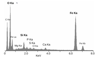
Energy-dispersive X-ray spectroscopy, sometimes called energy dispersive X-ray analysis or energy dispersive X-ray microanalysis (EDXMA), is an analytical technique used for the elemental analysis or chemical characterization of a sample. It relies on an interaction of some source of X-ray excitation and a sample. Its characterization capabilities are due in large part to the fundamental principle that each element has a unique atomic structure allowing a unique set of peaks on its electromagnetic emission spectrum. The peak positions are predicted by the Moseley's law with accuracy much better than experimental resolution of a typical EDX instrument.

X-ray spectroscopy is a general term for several spectroscopic techniques for characterization of materials by using x-ray radiation.
A microprobe is an instrument that applies a stable and well-focused beam of charged particles to a sample.

An electron microprobe (EMP), also known as an electron probe microanalyzer (EPMA) or electron micro probe analyzer (EMPA), is an analytical tool used to non-destructively determine the chemical composition of small volumes of solid materials. It works similarly to a scanning electron microscope: the sample is bombarded with an electron beam, emitting x-rays at wavelengths characteristic to the elements being analyzed. This enables the abundances of elements present within small sample volumes to be determined, when a conventional accelerating voltage of 15-20 kV is used. The concentrations of elements from lithium to plutonium may be measured at levels as low as 100 parts per million (ppm), material dependent, although with care, levels below 10 ppm are possible. The ability to quantify lithium by EPMA became a reality in 2008.

A scanning transmission electron microscope (STEM) is a type of transmission electron microscope (TEM). Pronunciation is [stɛm] or [ɛsti:i:ɛm]. As with a conventional transmission electron microscope (CTEM), images are formed by electrons passing through a sufficiently thin specimen. However, unlike CTEM, in STEM the electron beam is focused to a fine spot which is then scanned over the sample in a raster illumination system constructed so that the sample is illuminated at each point with the beam parallel to the optical axis. The rastering of the beam across the sample makes STEM suitable for analytical techniques such as Z-contrast annular dark-field imaging, and spectroscopic mapping by energy dispersive X-ray (EDX) spectroscopy, or electron energy loss spectroscopy (EELS). These signals can be obtained simultaneously, allowing direct correlation of images and spectroscopic data.

Focused ion beam, also known as FIB, is a technique used particularly in the semiconductor industry, materials science and increasingly in the biological field for site-specific analysis, deposition, and ablation of materials. A FIB setup is a scientific instrument that resembles a scanning electron microscope (SEM). However, while the SEM uses a focused beam of electrons to image the sample in the chamber, a FIB setup uses a focused beam of ions instead. FIB can also be incorporated in a system with both electron and ion beam columns, allowing the same feature to be investigated using either of the beams. FIB should not be confused with using a beam of focused ions for direct write lithography. These are generally quite different systems where the material is modified by other mechanisms.
Characterization, when used in materials science, refers to the broad and general process by which a material's structure and properties are probed and measured. It is a fundamental process in the field of materials science, without which no scientific understanding of engineering materials could be ascertained. The scope of the term often differs; some definitions limit the term's use to techniques which study the microscopic structure and properties of materials, while others use the term to refer to any materials analysis process including macroscopic techniques such as mechanical testing, thermal analysis and density calculation. The scale of the structures observed in materials characterization ranges from angstroms, such as in the imaging of individual atoms and chemical bonds, up to centimeters, such as in the imaging of coarse grain structures in metals.

Nestor J. Zaluzec is an American scientist and inventor who works at Argonne National Laboratory. He invented and patented the Scanning Confocal Electron Microscope. and the π Steradian Transmission X-ray Detector for Electron-Optical Beam Lines and Microscopes.
Aspex Corporation, founded in 1992, is a supplier of electron microscopy tools to researchers, developers and manufacturers working on Process control through automated scanning electron microscope and energy-dispersive X-ray spectroscopy.
Micro x-ray fluorescence (µXRF) is an elemental analysis technique that relies on the same principles as x-ray fluorescence (XRF). Synchrotron X-rays may be used to provide elemental imaging with biological samples. The spatial resolution diameter of micro x-ray fluorescence is many orders of magnitude smaller than that of conventional XRF. While a smaller excitation spot can be achieved by restricting x-ray beam using a pinhole aperture, this method blocks much of the x-ray flux which has an adverse effect on the sensitivity of trace elemental analysis. Two types of x-ray optics, polycapillary and doubly curved crystal focusing optics, are able to create small focal spots of just a few micrometers in diameter. By using x-ray optics, the irradiation of the focal spot is much more intense and allows for enhanced trace element analysis and better resolution of small features. Micro x-ray fluorescence using x-ray optics has been used in applications such as forensics, small feature evaluations, elemental mapping, mineralogy, electronics, multi-layered coating analysis, micro-contamination detection, film and plating thickness, biology and environment.
Ceramic petrography is a laboratory-based scientific archaeological technique that examines the mineralogical and microstructural composition of ceramics and other inorganic materials under the polarised light microscope in order to interpret aspects of the provenance and technology of artefacts.
The Rathgen Research Laboratory is a Research Institute of the Berlin State Museums under the auspices of the Prussian Cultural Heritage Foundation. It carries out cross-material conservation science, art technology and archaeometry studies of fine arts and cultural artifacts to determine composition, age and authenticity and provide advice on their restoration. It further conducts academic research on scientific issues concerning the care and preservation of monuments and archaeological sites. Founded in 1888 as the Chemical Laboratory of the Royal Museums in Berlin, it is the oldest museum laboratory in world and bears the name of its first director, Dr. Friedrich Rathgen.

Raimond Bernard René Castaing, also spelt as Raymond Castaing, was a French solid state physicist and inventor of various materials characterization methods. He was the founder of the French school of microanalysis and is referred to as the father of microanalysis.